
Signal Processing
Index 121
VHF_SWEPI_OSCILLATOR
Published:2009/7/24 2:22:00 Author:Jessie
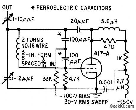
Voltage-tunable ferroelectric capacitors give tuning ratio of about 2 to 1 from 20 to 250 Mc and 1.5 to 1 from 250 to 400 Mc.-T. W. Butler, Jt., Ferroelectrics Tune Electronic Circuits, Electronics, 32:3, p 52-55. (View)
View full Circuit Diagram | Comments | Reading(478)
IONOSPHERIC_SOUNDER_PULSE_SIMULATOR
Published:2009/7/24 2:47:00 Author:Jessie

Generates long and short output pulses with positive and negative polarities, each adjustable in duration and amplitude. Small pulse can be moved through large pulse. Simulator is triggered at power-line frequency.-K. Perry, Back-Scatter Simulator Checks lonospheric Sounder Displays, Electronics, 35:25, p 50. (View)
View full Circuit Diagram | Comments | Reading(545)
ZENER_GENERATOR
Published:2009/7/2 3:39:00 Author:May
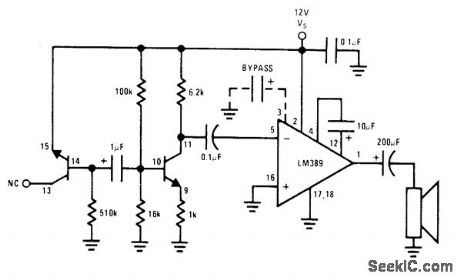
Uses National LM389 array having three transistors along with opamp. Application of reverse voltage to emitter of one grounded-base transistor breaks it down in avalanche mode to give action of zener diode. Reverse voltage characteristic, typically7.1 V, is used as noise source for amplification by second transistor and power opamp. Third transistor(notshown) can be used to gate noise generator if desired.- Audio Handbook, National Semiconductor. Santa Clara. CA. 1977. p 4-33-4-37. (View)
View full Circuit Diagram | Comments | Reading(815)
168_GHz_03_W_oscillator_20_V_supply
Published:2009/7/24 2:31:00 Author:Jessie
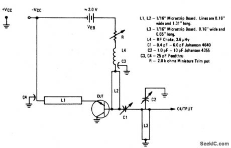
The electrical characteristics for the 2N5108 shown in this circuit are given in Fig.2-20B.Those not familiar with microstrip techniques(for L1,L2,and L3)should read the many Motorola publications, such as AN548A and AN555. (View)
View full Circuit Diagram | Comments | Reading(773)
50_MHz_40_W_transmitter_125_V_supply
Published:2009/7/24 2:47:00 Author:Jessie
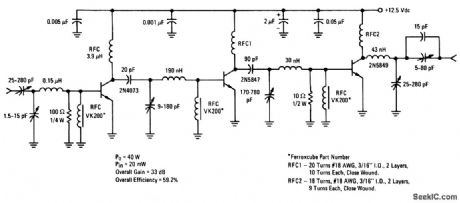
This circuit provides 40 W of output power with 20-mW input power in the 50-MHz band. (View)
View full Circuit Diagram | Comments | Reading(1257)
TEMPERATURE_COMPENSATING_VFO_CIRCUITS
Published:2009/7/24 2:40:00 Author:Jessie

Here are two ways in which adjustable temperature compensation can be achieved: (a) with a differential capacitor, and (b) with two conventional trimmers. (View)
View full Circuit Diagram | Comments | Reading(721)
NE602_COLPITTS_VFO
Published:2009/7/24 2:35:00 Author:Jessie
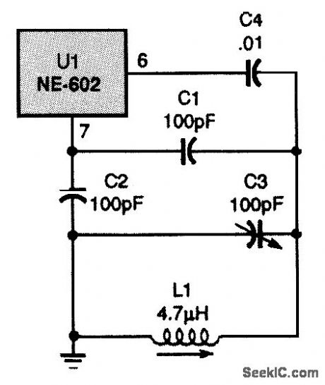
In this Colpitts variable-frequency oscillator (VFO), an inductor/capacitor combination is used to set the frequency. (View)
View full Circuit Diagram | Comments | Reading(994)
STABLE_HF_VFO
Published:2009/7/24 2:34:00 Author:Jessie

This circuit is a Hartley oscillator, as identified by the fact that the feedback to the JFET transistor (Q1) is supplied by a tap on the tuning inductance (L1). The position of the tap is usually between 10 and 35 percent of the total coil length. A buffer amplifier is included, and it provides two basic functions: It boosts the low output power from the oscillator to a higher level and it isolates the oscillator from changing load impedances. The main tuning capacitor (C1) is a 100-pF air-dielectric variable unit of heavy-duty double-bearing construction, The trimmer (C2) is used to set the exact frequency, especially when using a dial that must be calibrated. Note that several of the fixed capacitors are indicated as being NPO ceramic-disk, polystyrene, or silvered mica (in order of preference). Also notice that a voltage regulator (U1) serves the oscillator. This generates very little heat; nonetheless, it is still a good idea to mount the regulator away from the actual oscillator circuit. The small trimmer capacitors (C2 and C4) are air-dielectric types, rather than mica or ceramic. The purpose of C4 is to provide dc blocking to the transistor-gate circuit. It has such a small value because we want to lightly load the LC-tuned circuit. That trimmer is adjusted from a position of minimum capacitance (i.e., with the rotor plates completely unmeshed from the stator plates), and is then advanced to a higher capacitance as the oscillator is turned on and off. The correct position is the lowest value that allows the oscillator to start immediately every time that power is applied.
(View)
View full Circuit Diagram | Comments | Reading(3319)
NOISE_GENERATOR
Published:2009/7/2 2:42:00 Author:May
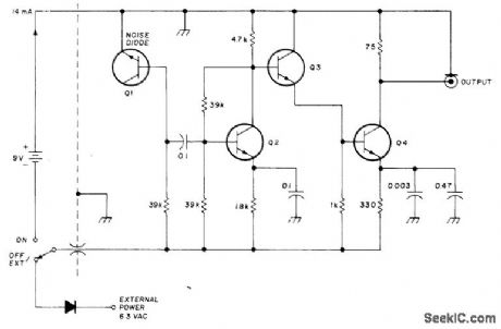
Used with communication receiver to measure Q of tuned circuit without disconnecting circuit. Noise diode gives constant noise signal strength over wide frequency band. so frequency response of tuned circuit can be observed with receiver. Q is calculated after using S-meter of receiver to find -6 dB bandwidth. AII transistors are 2N2368; select noisiest for Q1. Article covers test setup for measuring Q.-R. C. Marshall. Q Measure-ment and More. Ham Fladio. Jan. 1977. p 49-51. (View)
View full Circuit Diagram | Comments | Reading(564)
VFO_AGC_CIRCUIT
Published:2009/7/24 2:39:00 Author:Jessie
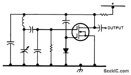
This is a possible simple AGC system for use with a Vackar oscillator, which should be an improvement over a diode connected directly between gate and source. D1 can be any good-quality RF silicon diode. (View)
View full Circuit Diagram | Comments | Reading(1056)
SPEECH_SIMULATOR
Published:2009/7/24 2:38:00 Author:Jessie
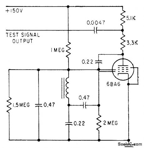
Electron-coupled 1-kc Colpitts oscillator is modified to hunt at approximately 10 cps. Serves as source of fluctuating-amplitude audio lone, to simulate speech in narrow spectrum region.-H. Schwarzlander, Intelligibility Evaluation of Voice Communications, Electronics, 32:22, p 88-91. (View)
View full Circuit Diagram | Comments | Reading(540)
500_MHz_20_mW_oscillator_10_V_supply
Published:2009/7/24 2:38:00 Author:Jessie
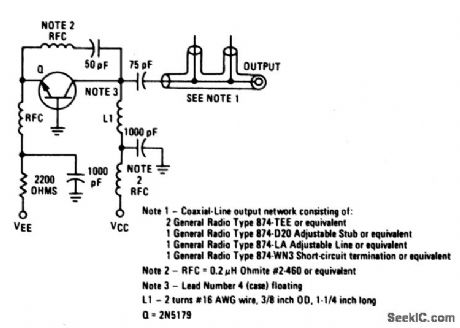
The electrical characteristics for the 2N5179 shown in this circuit are given in Fig.2-24B. (View)
View full Circuit Diagram | Comments | Reading(809)
CLUTTER_GENERATOR
Published:2009/7/24 2:38:00 Author:Jessie
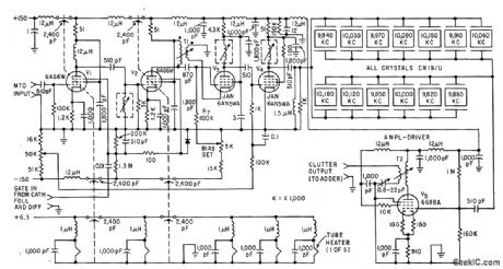
Simulates radar clutter received by rotating antenna on 550-mph aircraft, for checking airborne moving-target indicator on ground. Clutter is produced by ringing bank of closely spaced crystals and allowing resulting frequencies to beat together to produce jagged clutter return that decoys with range.-H. Lobenstein and A. R. Dial, Radar-Return Simulator Tests Moving-Target Indicators, Electronics, 33:49, p 58-60. (View)
View full Circuit Diagram | Comments | Reading(662)
COLPITTS_VFO
Published:2009/7/24 2:37:00 Author:Jessie


Three capacitors (C1, C2, and C3) are used in this NE602AN IC Colpitts oscillator circuit, rather than two, because of the need for dc blocking. The values of the components are as follows:
C1,C2,C3≈2400/ƒ(MHz)C4=1/[(2πƒ)2 L1]L1≈7/ƒ(MHz)microhenries (View)
View full Circuit Diagram | Comments | Reading(1440)
PINK_NOISE_GENERATOR
Published:2009/7/2 2:06:00 Author:May
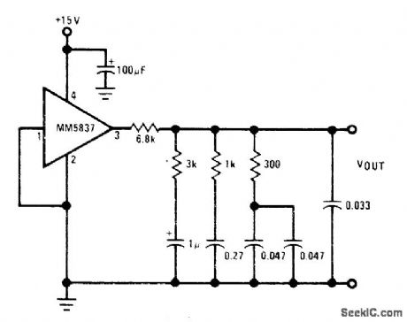
Uses MM5837 broadband white-noise generator with -3 dB per octave filter from 10 Hz to 40 kHz to give pink-noise output having flat spectral distribution over entire audio band from 20 Hz to 20 kHz.Output is about 1 V P-P of pink noise riding on 8.5-VOC level. Used as controlled source of noise for adjusting octave equalizer to optimum settings for specific listening area.- Audio Handbook. National Semiconductor. Santa Clara. CA. 1977. p 2-53-2-59. (View)
View full Circuit Diagram | Comments | Reading(3848)
CLAPP_JFET_VFO
Published:2009/7/24 2:41:00 Author:Jessie
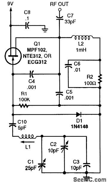
The JFET VFO circuit shown here can be identified as a Clapp oscillator by its series-tuned LC network. This circuit as shown can be used from 0.5 to 7 MHz. (View)
View full Circuit Diagram | Comments | Reading(739)
DATA_COUPLER_WITH_ISOLATION
Published:2009/7/2 2:04:00 Author:May

Length of fiber or polystyrene rod determines amount of voltage isolation provided between digital or analog signal input and Fairchild FPT 100 photodetector driving Optical Electronics 9720 opamp having 100-mA output for driving cables, relays, or loudspeakers. LED can be Monsanto MV50 handling up to 200 mA. Output of opamp is zero for no light. Pulse-duration modulation should be used for transmission of analog data.- High Voltage Optically Isolated Data Coupler, Optical Electronics, Tucson, AZ,Application Tip 10266. (View)
View full Circuit Diagram | Comments | Reading(703)
STAIRCASE_COUNTER
Published:2009/7/24 2:57:00 Author:Jessie
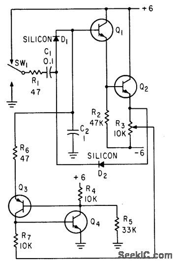
Q1-Q2 serve as boot-strap amplifier for voltage on storage capacitor C2. Each incoming pulse transfers charge increment from C1 to C2. Reliable counts as large as Ion are easily obtained.-N. C. Hekimian, PNP-NPN CIRCUITS: New Look at a Familiar connection, Electronics, 35:47, p 42-46. (View)
View full Circuit Diagram | Comments | Reading(515)
WIDE_RANGE_STAIRCASE_GENERATOR
Published:2009/7/24 2:57:00 Author:Jessie
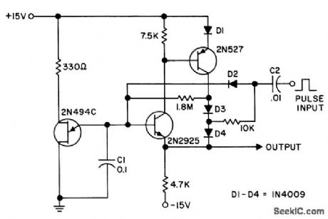
Has high input impedance und low output impedance, to reduce droop in output voltage between pulses. Staircase is generated by pump D2-C2, which is boostrapped on output to maintain equal amplitude on each step. Circuit values shown give 10 steps with 12-V input pulse.- Transistor Manual, Seventh Edition, General Electric Co., 1964, p 345. (View)
View full Circuit Diagram | Comments | Reading(804)
50_MHz_CRYSTAL
Published:2009/7/2 1:07:00 Author:May

Uses microtransistor as oscillator handling 100-mW input power and giving 40-50% efficiency. Article covers construction with microcomponents and gives other microtransistor circuits for low-power amateur radio use and possible bugging applications.-B. Hoisington, Introduction to Microtransistors, 73 Magazine, Oct. 1974, p 24-30. (View)
View full Circuit Diagram | Comments | Reading(724)
| Pages:121/195 At 20121122123124125126127128129130131132133134135136137138139140Under 20 |
Circuit Categories
power supply circuit
Amplifier Circuit
Basic Circuit
LED and Light Circuit
Sensor Circuit
Signal Processing
Electrical Equipment Circuit
Control Circuit
Remote Control Circuit
A/D-D/A Converter Circuit
Audio Circuit
Measuring and Test Circuit
Communication Circuit
Computer-Related Circuit
555 Circuit
Automotive Circuit
Repairing Circuit