
Signal Processing
Index 139
SAWTOOTH_GENERATOR
Published:2009/6/23 4:35:00 Author:May

A sawtooth waveform generator circuit using a 555 IC is shown. The IC is connected in an astable oscillator circuit with the majority of the output contained in the positive portion of the cy-cle. The negative output is a very brief pulse.Capacitor C2 charges through R3 in a positive direction during the time that the IC's output (at pin 3) is high. When the output goes negative, C2 is rapidly discharged through Dl and the IC's out-put.Peak-to-peak sawtooth output is about 1 V. The linearity of this circuit is best when R3 is as large as possible. The oscillator's frequency is about 200 Hz and can be increased by lowering either the value of R1 or C1 to decrease the frequency, increase the values of those components. (View)
View full Circuit Diagram | Comments | Reading(0)
SIMPLE_TLO82_VCO
Published:2009/6/23 4:32:00 Author:May

This circuit uses a dual operational amplifier (TL082) to form a voltage-controlled oscillator (VCO). With the component values shown, the output-frequency range is 100 Hz to 10 kHz when the input control voltage is between 0.05 and 10 V. (View)
View full Circuit Diagram | Comments | Reading(0)
SHORTWAVE_CONVERTERS_FOR_SCANNERS
Published:2009/6/23 4:39:00 Author:Jessie
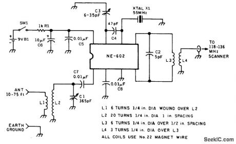
The AM aircraft band at 118 to 136 MHz is used in this converter design as an IF output The second harmonic ofthe 55 MHz crystal(110 MHz) mixes with the shortwave input of 8 to 36 MHz.AnNE602 IC IS used for the mlxer Sensitivity IS about 3μV. If desired,a crystal tuning circuit for finetuning can be obtained ustng a varactor (View)
View full Circuit Diagram | Comments | Reading(1926)
SCANNER_SILENCER
Published:2009/6/23 4:38:00 Author:Jessie
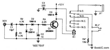
When a scanner is used at amateur radio or CB stations, the scanner sometimes picks up trans-mitted signal and howls or squeals. When RF is detected, Q1 tums on, energizing K1 and discon-necting the scanner speakers. SO1 is connected to the transmit antenna lead via a tee fitting. C1 is optimum for 5- to 10-W 30-MHz use. For higher power or higher frequencies, reduce C1 to as low as needed. If C1 is so small as to be impractical, R1 can be shunted with a 10- or 22-pF capacitor, as needed. (View)
View full Circuit Diagram | Comments | Reading(646)
FM_SCANNER_NOISE_SQUELCH
Published:2009/6/23 4:37:00 Author:Jessie
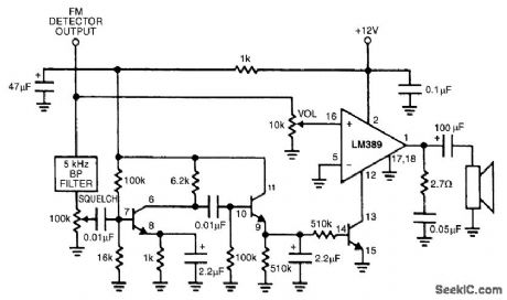
The LM389 is operated in the cut-off mode with pin 12 grounded via one of the internal transistors. A sample of detected noise is taken through a 5-kHz filter. Upon reception of signal, the detec-tor output quiets, and noise level drops. This increases impedance at pin 12 of the LM389, causing audio to be passed. The three transistors are part of the LM389. (View)
View full Circuit Diagram | Comments | Reading(1651)
MODEL_RAILROAD_TRACK_CONTROL_SIGNAL
Published:2009/6/23 4:30:00 Author:Jessie

When a train passesS1 (a red switch), a small magnet glued to the underside operates Sl and causes UI to generate a pulse, activating relay K1 and changing the signal from green to red. After a time determined by RI and C1 (see table), the relay de-energizes and the signal goes back to green. (View)
View full Circuit Diagram | Comments | Reading(1484)
DUAL_TONE_GENERATOR_FOR_AUDIO_SERVICING
Published:2009/6/23 3:34:00 Author:May

This dual-tone generator can insert a distinctive tone in the audio section of a circuit under test.That way, you can work your way back from the speaker, stage-by-stage, to locate a faulty section. (View)
View full Circuit Diagram | Comments | Reading(1375)
POSITIVE_FEEDBACK_CABLE_TERMINATOR
Published:2009/6/23 3:18:00 Author:Jessie

Positive feedback along with a series output resistor can provide a controlled output impedance from an op-amp circuit. The circuit is useful when driving coaxial cables that must be terminated at each end in their characteristic impedance, which is often 50Q. Adding a 50-Q series resistor on the op amp's output obviously reduces the available signal swing. (View)
View full Circuit Diagram | Comments | Reading(1033)
FM_MODULATOR
Published:2009/6/23 3:08:00 Author:Jessie

The FM modulator is built with a Motorola MC1648P oscillator. Two varactors, Motorola MV209, are used to frequency modulate the oscillator. The 5000-Ω potentiometer is used to bias the varactors for best linearity. The output fre-quency of approximately 100 MHz can be ad-justed by changing the value of the inductor. The output frequency can vary as much as 10 MHz on each side. The output level of the modulator is -5 dBm. In this prototype, the varactor bias was 7.5 V for best linearity; but this could be different with other varactors. (View)
View full Circuit Diagram | Comments | Reading(2553)
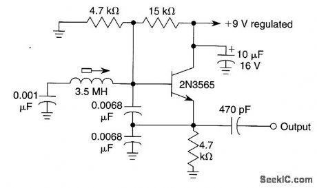
HARTLEY_OSCILLATOR
Published:2009/6/23 2:35:00 Author:May
This circuit uses a tapped inductor in a Hartley oscillator circuit. The tap is generally at 25 to 35% total tums in most instances. (View)
View full Circuit Diagram | Comments | Reading(925)
TUNED_COLLECTOR_OSCILLATOR
Published:2009/6/23 2:34:00 Author:May
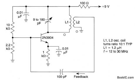
View full Circuit Diagram | Comments | Reading(921)
CLAPP_OSCILLATOR_FOR_100_kHz
Published:2009/6/23 2:32:00 Author:May
This Colpitts oscillator is very stable and usable where good stability is needed, but crystal control is not desirable. It is capable of 1 part in 104 to 105 with good-quality components. (View)
View full Circuit Diagram | Comments | Reading(898)
COLPITTS_OSCILLATOR
Published:2009/6/23 2:31:00 Author:May
In this circuit, the oscillator is free-running. (View)
View full Circuit Diagram | Comments | Reading(0)
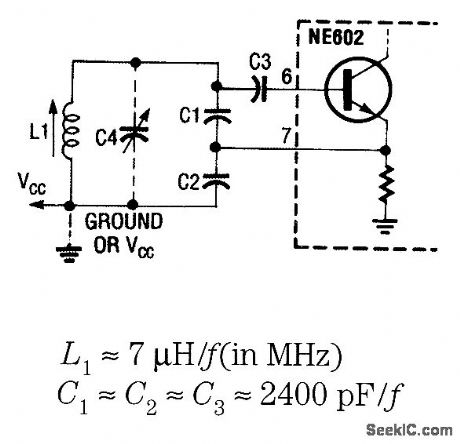
OSCILLATOR_CIRCUITS
Published:2009/6/23 2:31:00 Author:May

These are methods of using an NE602 with a tunable VFO. (View)
View full Circuit Diagram | Comments | Reading(1190)
“UNIVERSAL”VFO
Published:2009/6/23 2:30:00 Author:May

Figure 63-16A shows the basic circuit for the VFO, except for the tuning circuits (which are shown in Fig. 63-16B). Transistor Q1 is a junction field-effect transistor (JFET) oscillator stage. The device to use at Q1 includes MPF-102, 2N4416, and the replacement devices from the popular lines of service parts e.g., ECG and NTE).Two different oscillator configurations can be accommodated by this design (i.e., both Clapp and Colpitts oscillators can be built). Both oscillators are the same from point A in Fig. 63-16C forward, and both depend on a capacitor voltage-divider feedback network. The Clapp oscillator (Fig. 63-16A) is series-tuned and the Colpitts oscillator is parallel-tuned (Fig. 63-16B).The dc voltage supplied to the oscillator transistor (Q1) is voltage-regulated. The voltage regu-lator can be any 78Lxx series from 78LO5 to 78LO9. (View)
View full Circuit Diagram | Comments | Reading(3179)
Sine wave signal source with stable output
Published:2011/7/28 3:24:00 Author:Ecco | Keyword: Sine wave , signal source , stable output

Figure shows the sine wave signal source with stable output. First using of an op amp comparator could produce a constant 60Hz square wave. The output end of comparator is connecting to a pair of 6.2V back connecting zener diodes. The following is a two-stage Sallen-key low pass filter, which canfilter out all harmonics. Capacitive coupling amplifier cuts off the DC component produced by zener diode which is not equal in circuit, it also make compensation for filter loss, and the precise calibration of the output amplitude can reach l0V peak. The result is that it gets a high stable 60Hz sine wave voltage with low distortion. In the case of constant ambient temperature, power supply voltage range is 90 ~ 135V, the sine wave output voltage rate of change is less than 5mV.
(View)
View full Circuit Diagram | Comments | Reading(792)
Digital sine wave generator
Published:2011/7/28 3:23:00 Author:Ecco | Keyword: Digital , sine wave, generator

Digital sine wave generator is shown as the chart. It consists of analog digital converter (4018B) and a fixed filter (MAX29X). One part of the clock pulse input CP drives MAX29X filter, and the others makes fractional frequency by the first 10-bit counter (4018B) and then by the second l0-bit counter. The output step wave becomes smooth sine wave by R5 and Cl, and then it is output after filtered by the filter. The output frequency changes with the input of clock, the relationship is fout = fin/l00.
(View)
View full Circuit Diagram | Comments | Reading(0)
DARLINGTON_TRANSISTOR_OSCILLATOR
Published:2009/6/23 2:23:00 Author:May

This oscillator uses a very large capacitance-to-inductance ratio. L1 is a one-tum coil consisting of a loop of #12 wire 12 in diameter. This circuit is useful for metal detectors, etc., where a loop antenna is used. (View)
View full Circuit Diagram | Comments | Reading(0)
GROUNDED_BASE_TUNED_COLLECTOR_OSCILLATOR_FOR_AM_BROADCAST_BAND
Published:2009/6/23 2:20:00 Author:May

View full Circuit Diagram | Comments | Reading(0)
VLF_LC_OSCILLATOR
Published:2009/6/23 2:19:00 Author:May

The VLF oscillator uses a large toroid coil as the frequency-determining component and a 2N5485 FET as the active device. R3 is used as a feedback control and also by running the circuit with slightly less feedback than needed for oscillation, can serve as a regenerative amplifier or detector. (View)
View full Circuit Diagram | Comments | Reading(2480)
| Pages:139/195 At 20121122123124125126127128129130131132133134135136137138139140Under 20 |
Circuit Categories
power supply circuit
Amplifier Circuit
Basic Circuit
LED and Light Circuit
Sensor Circuit
Signal Processing
Electrical Equipment Circuit
Control Circuit
Remote Control Circuit
A/D-D/A Converter Circuit
Audio Circuit
Measuring and Test Circuit
Communication Circuit
Computer-Related Circuit
555 Circuit
Automotive Circuit
Repairing Circuit