
Signal Processing
Index 132
PULSE_GENERATOR_1
Published:2009/6/25 4:43:00 Author:May

View full Circuit Diagram | Comments | Reading(1098)
UNIJUNCTION_TRANSISTOR_PULSE_GENERATORS
Published:2009/6/25 4:42:00 Author:May
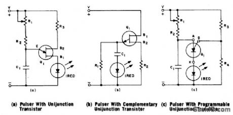
View full Circuit Diagram | Comments | Reading(722)
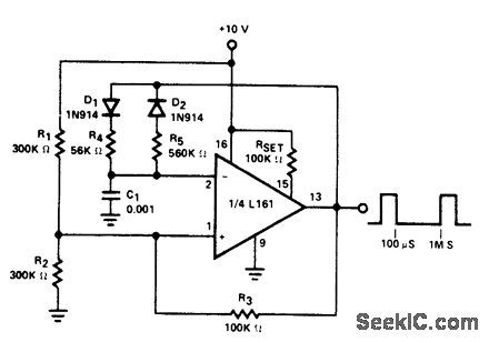
PROGRAMMABLE_PULSE_GENERATOR
Published:2009/6/25 4:42:00 Author:May

Fast rlse and fall times requlre the use of high speed switching transistors for the differential patr,Q4 and Q5.Linear ramps and slnewaves may be generated by the appropriatereference input. (View)
View full Circuit Diagram | Comments | Reading(0)
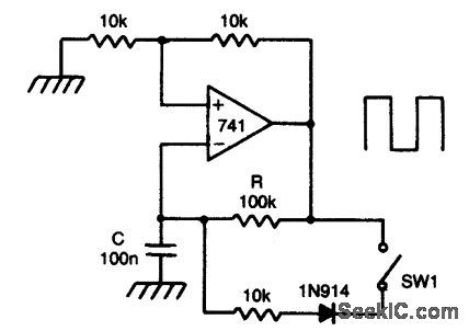
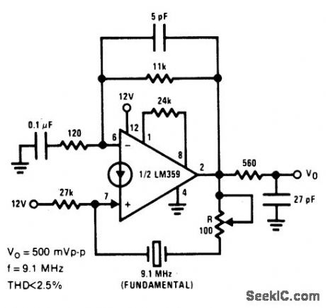
SINGLE_OP_AMP_OSCILLATOR
Published:2009/6/25 4:40:00 Author:May

This circuit has a Schmitt trigger and in-tegrator built around one op amp. Timing is controlled by the RC network. Voltage at the inverting input follows the RC charging expo-nential within the upper and lower hysteresis levels. By closing the switch SWt, the dis-charge time of the capacitor becomes ten times as fast as the rise time. Thus a square wave with an 10:1 mark space ratio is generated. (View)
View full Circuit Diagram | Comments | Reading(1215)
PULSE_GENERATOR
Published:2009/6/25 4:37:00 Author:May

The duty cycle ofthe output pulse is equalto R4/(R4+R5)×100%.For duty cycles ofless than 50%,D1 can be eliminated and R2raised according to the following formula∶
R4(actual)=
R4c(eff) IS the effective value ofR4 in the circuitand R4(actual)IS the actual value used;R4(ac-tual)will always be larger than R4(eff). (View)
View full Circuit Diagram | Comments | Reading(0)
INJECTOR_TRACER
Published:2009/6/25 4:06:00 Author:Jessie

The unit has a separate amplifier and oscillator section allowing them to be used sepa-rately if need be. The injector is a multivibrator running at 1 kHz, with R5 and R6 dividing down the output to a suitable level (≈1V). The tracer is a single-stage amplifier that drives the high impedance earpiece. C4 decouples the input. (View)
View full Circuit Diagram | Comments | Reading(1653)
SIGNAL_INJECTOR_TRACER
Published:2009/6/25 4:04:00 Author:Jessie

The injector is a CMOS oscillator with period approximately equal to 1.4 x C1 x R2 seconds. The values are given for 1 kHz opera-tion. Resistors R3 and R4 divide the output to 1 V. Whereas the oscillator employs the gates in their digital mode, the tracer used them in a linear fashion by applying negative feedback from output to input. They are used in much the same way as op amps. The circuit uses positiveground. It offers an advantage at the earphone output because one side of the earphone must be connected to ground via the case. Use of a positive ground allows the phone to be driven by the two N-channel transistors inside the CD4001 which are arranged in parallel and are thus able to handle more current for better volume. (View)
View full Circuit Diagram | Comments | Reading(3127)
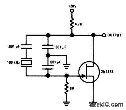
PIERCE_HARMONIC_OSCILLATOR(100_MHz)
Published:2009/6/25 3:10:00 Author:May

Circuit Notes
The output resistance of the transistor's collector, together with the effective value of C1, provides an RC phase lag of 30-500. The crystal normally oscillates slightly above series resonance, where it is both resistive and inductive. Above series resonance, the crys-tal's internal impedance (resistive and induc-tive) together with C2 provides an RLC phase lag of 130-1500. The transistor inverts the sig-nal, providing a total of 3600 of phase shift around the loop. Inductor L1 is selected to resonate with C1 at a frequency between the crystal's desired harmonic and its next lower odd harmonic. Inductor L1 offsets part of the negative reactance of C1 at the oscillation fre-quency. (View)
View full Circuit Diagram | Comments | Reading(1201)
CMOS_OSCILLATOR_1_MHz_4_MHz
Published:2009/6/25 3:07:00 Author:May

View full Circuit Diagram | Comments | Reading(659)
JFET_PIERCE_CRYSTAL_OSCILLATOR__
Published:2009/6/25 3:04:00 Author:May


Circuit Notes TheJFET Pierce crystal oscillator allowsa wide frequency range of crystals to be usedwithout circuit modification,Since the JFETgate does not load the crystal, good Q IS maln-tained,thus lnsurlng good frequency stability. (View)
View full Circuit Diagram | Comments | Reading(1014)
STABLE_LOWFREQUENCY_CRYSTAL_OSCILLATOR
Published:2009/6/25 3:02:00 Author:May
Circuit Notes This Colpitts-crystal oscillator IS ideal forlow frequency crystal oscillator circuits。 Ex-cellent stability is assured because the 2N3823 JFET circuit loading does not vary with tem-perature. (View)
View full Circuit Diagram | Comments | Reading(980)
CRYSTAL_CONTROLLED___SINE_WAVE_OSCILLATOR_
Published:2009/6/25 3:00:00 Author:May
View full Circuit Diagram | Comments | Reading(727)
TTL_COMPATIBLE_CRYSTAL_OSCILLATOR
Published:2009/6/25 2:57:00 Author:May

Circuit NotesAdjust RI for about 2 volts at the output ofthe first gate,Adjust C1 for best output (View)
View full Circuit Diagram | Comments | Reading(686)
STANDARD_CRYSTALOSCILLATOR_FOR_1_MHz
Published:2009/6/25 2:55:00 Author:May

View full Circuit Diagram | Comments | Reading(527)
INTERNATIONAL_CRYSTAL_OF_1_HI_OSCILLATOR
Published:2009/6/25 2:55:00 Author:May
Circuit NotesInternational Crystal OF-1 HI oscillator circuit for third-overtone crystals. The circuit does not requlre inductors. (View)
View full Circuit Diagram | Comments | Reading(653)
BUTLER_APERIODIC_OSCILLATOR
Published:2009/6/25 2:50:00 Author:May
Circuit Notes
This circuit works well in the range of 50 kHz to 500 kHz. Slight component modifica-tions are needed for higher frequency opera-tion. For operation over 3000 kHz, select a transistor that provides moderate gain (in the 60 to 150 range) at the frequency of operation and a gain-bandwidth product of at least 100 MHz. (View)
View full Circuit Diagram | Comments | Reading(547)
PIERCE_OSCILLATOR
Published:2009/6/25 2:36:00 Author:May
Circuit Notes
The oscillator transistor is Q1, and the crystal is placed between the collector and base. Feedback is improved by the use of the collector-emitter capacitor C2. Transistor Q2 is used as an output buffer. (View)
View full Circuit Diagram | Comments | Reading(0)
CRYSTAL_CONTROLLED_OSCILLATOR
Published:2009/6/25 2:35:00 Author:May


Circuit Notes
This circuit oscillates without the crystal. With the crystal in the circuit, the frequency will be that of the crystal. The circuit has good starting characteristics even with the poorest crystals. (View)
View full Circuit Diagram | Comments | Reading(0)
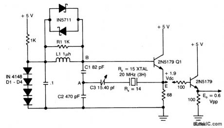
COLPITTS_OSCILLATOR
Published:2009/6/25 2:32:00 Author:May

Circuit Notes
This circuit will operate with fundamental-mode crystals in the range of 1MHz to 20 MHz,Feedback is controlled by capacitor voltage divider C2/C3.The rfvoltageacross the emitter resistor provides the basic feedback signal. (View)
View full Circuit Diagram | Comments | Reading(0)
BUTLER_EMITTER_FOLLOWER_OSCILLATOR(20_MHz)
Published:2009/6/25 2:26:00 Author:May
View full Circuit Diagram | Comments | Reading(0)
| Pages:132/195 At 20121122123124125126127128129130131132133134135136137138139140Under 20 |
Circuit Categories
power supply circuit
Amplifier Circuit
Basic Circuit
LED and Light Circuit
Sensor Circuit
Signal Processing
Electrical Equipment Circuit
Control Circuit
Remote Control Circuit
A/D-D/A Converter Circuit
Audio Circuit
Measuring and Test Circuit
Communication Circuit
Computer-Related Circuit
555 Circuit
Automotive Circuit
Repairing Circuit