
Signal Processing
Index 128
Keyed_oscillator
Published:2009/7/24 6:03:00 Author:Jessie

In this circuit, one timer section of an XR-L556 is operated in the free-running mode, and is keyedon and off by the other section. The circuit output (timer 2) appears as a tone burst, whose frequency is set by RA, RB, and C2, and whose duration is set by R1 and C1. EXAR Corporation Databook, 1990, p. 5-222. (View)
View full Circuit Diagram | Comments | Reading(697)
Sequential_timing_delayed_one_shot
Published:2009/7/24 6:01:00 Author:Jessie
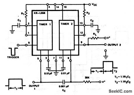
In this circuit, the output of one timer section triggers the other section so that the output of T2 is delayed from the initial trigger at pin 6 by a time delay of T1. Both T1 and T2 are set by values of external components, as shown. EXAR Corporation Databook, 1990 , p. 5-221. (View)
View full Circuit Diagram | Comments | Reading(535)
Independent_time_delay
Published:2009/7/24 6:00:00 Author:Jessie
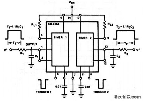
This circuit uses both sections of an XR-L556 dual timer to produce two independent time delays. Each section is used separately in the monostable mode to produce respective time delays T1 and T2. EXAR Corporation Databook, 1990 , p. 5-221. (View)
View full Circuit Diagram | Comments | Reading(517)
Astable_free_running
Published:2009/7/24 5:59:00 Author:Jessie
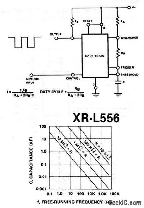
This circuit uses one section of an XR-L556 dual timer. Output frequency and duty cycle are set by C and R (Fig. 5-12B). Notice that R=RA + 2RB (Fig. 5-12B). EXAR Corporaton Databook, 1990, p. 5-218/5-221. (View)
View full Circuit Diagram | Comments | Reading(509)
Monostable_one_shot
Published:2009/7/24 5:57:00 Author:Jessie
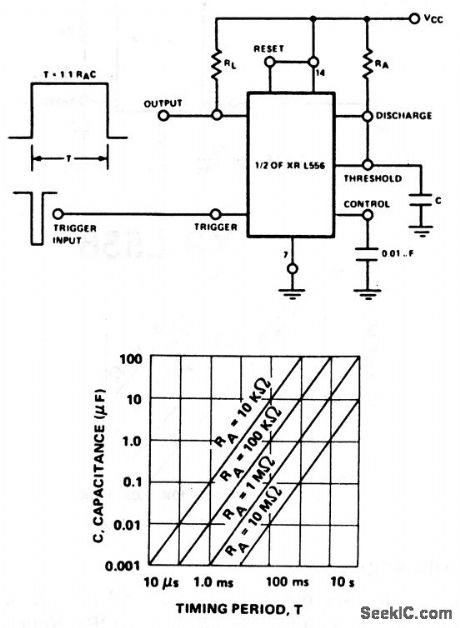
This circuit uses one section of an XR-L556 dual timer. Duration of the output pulse is set by C and RA (Fig. 5-11B). RL should equal the load being driven. EXAR Corporation Databook, 1990 , p. 5-218/5-220. (View)
View full Circuit Diagram | Comments | Reading(531)
Square_wave_oscillator
Published:2009/7/24 5:47:00 Author:Jessie
This circuit uses only one section of an LP165/365 comparator, and produces square waves at a frequency that is determined by the values of R and C, as shown. Raytheon Linear Integrated Circuts, 1989, p. 5-42. (View)
View full Circuit Diagram | Comments | Reading(1)
Crystal_controlled_oscillator
Published:2009/7/24 5:46:00 Author:Jessie

This circuit uses only one section of an LP165/365 comparator,and produces pulses at 100 kHz using the values shown, with a single supply. Raytheon Linear Integrated Circuts, 1989, p. 5-42. (View)
View full Circuit Diagram | Comments | Reading(1856)
Crystal_stabilized_relaxation_oscillator
Published:2009/7/24 7:50:00 Author:Jessie
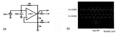
This circuit shows an LT1011 connected as a simple relaxation oscillator with crystal control. Figure 5-28B shows the corresponding waveforms. Waveform A is taken from the inverting ( -) input of the LT1011, while waveform B is taken from the LT1011 output. Linear Technology Corporation. Linear Appications Handbook, 1990, p. AN12-3, -2. (View)
View full Circuit Diagram | Comments | Reading(633)
Simple_clock_oscillators
Published:2009/7/24 7:48:00 Author:Jessie
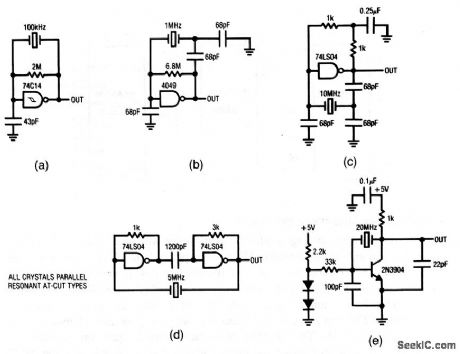
These circuits show four basic clock oscillators composed of digital IC gates, and a discrete-component oscillator, all of which are well suited as clock sources. Notice that the diodes used in the discrete-component oscillator can be 1N4148s or equivalent. Linear Technology Corporation, Linear Applications Handbook, 1990, p. AN12-2. (View)
View full Circuit Diagram | Comments | Reading(1090)
High_purity_sine_wave_generator
Published:2009/7/24 7:46:00 Author:Jessie

By combining a MAX270 4th-order low-pass filter, a 74HC163 counter, and an 8-channel analog MUX, high-purity 1- to 25-kHz sine waves are generated with a THD of less than -80 dB. The low-pass filter is set to the desired frequency and a clock 8 times the sine frequency is applied to the 74HC163 counter. The MAX270 uncommitted op amp sets the filter output level. Gain accuracy is set by the MAC270 gain at the corner frequency, which is guaranteed between -2.4 and -3.6 dB at 1 kHz. The 100-kΩ potentiometer provides gain control if desired. Two resistor dividers provide the input voltages that are required at the MUX inputs. When the MUX switches through channels 0 to 7, an 8-times oversampled staircase approximation of a sine wave is generated. Compared with a square wave, the oversampled waveform greatly reduces smoothing-filter requirements by pushing the first significant harmonic out to 7 times the fundamental. All higher-order harmonics are filtered to below -80 dB by the MAX270. Maxim , 1992, Applications and Product Highlights, p. 7-7. (View)
View full Circuit Diagram | Comments | Reading(1569)
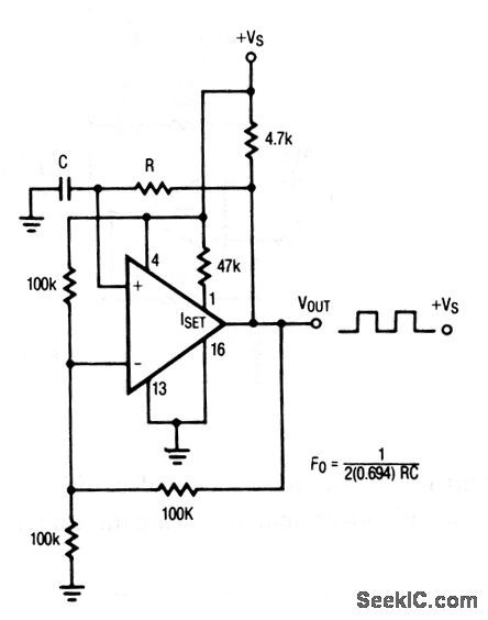
15_V_powered_temperature_compensated_crystal_oscillator
Published:2009/7/24 7:44:00 Author:Jessie
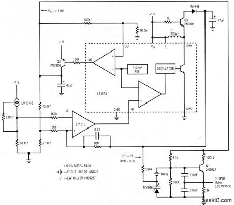
This fully temperature-compensated oscillator is operated from a 1.5-V source (single battery) and draws only 230-μA current, making the circuit ideal for portable high-accuracy clocks, survival radios, and secure communications. Linear Technology Corporation, 1991, AN45-14. (View)
View full Circuit Diagram | Comments | Reading(518)
Quartz_stabilized_4_kHz_oscillator_with_9_ppm_distortion
Published:2009/7/24 7:40:00 Author:Jessie

A spectrally pure sine-wave oscillator is required for data converter, filter, and audio testing. This oscillator has less than 9 ppm (0.0009%) distortion in the 10-Vpp output. The circuit is adjusted for minimum distortion by adjusting the 50-kΩ potentiometer while monitoring the A3 output with a distortion analyzer. This trim sets the voltage across the photocell to the optimum value for lowest distortion. Linear Technology Corporation, 1991, AN45-12. (View)
View full Circuit Diagram | Comments | Reading(620)
HIGH_DRIVE_OSCILLATOR_FLSHER
Published:2009/6/30 23:34:00 Author:May

The driver in the package is connected as a Schmitt trigger oscillator (A) where R1 and R2 are used to generate hysteresis. R3 and C are the inverting feedback timing elements and R4 is the pull-down load for the first driver. Because of its current capability, the circuit can be used to drive an array of LEDs or lamps. If resistor R4 is replaced by an LED (plus a current limiting resistor), the circuit becomes a double flasher with the 2 LEDs flashing out of phase (B). (View)
View full Circuit Diagram | Comments | Reading(587)
LOW_FREQUENCY_OSCILLATOR_FLASHER
Published:2009/6/30 23:29:00 Author:May

Electrolytic capacitors are unnecessary to generate a 1 cps frequency. As an scs triggers on, the 0.2 μF commutating capacitor turns off the other one and charges its gate capacitor to a negative potential. The gate capacitor charges towards 24 volts through 20 M retriggering its scs. Battery power is delivered to the load with 88% efftciency.The 20 M resistors can be varied to change prf or duty fact (View)
View full Circuit Diagram | Comments | Reading(676)
2_MHz_CRYSTAL_USING_CMOS_PAIR
Published:2009/6/30 23:13:00 Author:May

One CMOS transistor pair from CA3600E array is connected with feedback pinetwork to glve sta-ble oscilIator performance with 2-MHz crystal.Low power drain makes circuit ideal for use in digital clocks and watches.- Linear Integrated Circuits and MOS/FET's, RCA Solid State Divi-sion, Somerville, NJ, 1977, p 280. (View)
View full Circuit Diagram | Comments | Reading(647)
Vpp_GENERATOR_FOR_EPROMS
Published:2009/6/30 22:34:00 Author:May

View full Circuit Diagram | Comments | Reading(572)
RE_OSCILLATOR
Published:2009/6/30 3:05:00 Author:May

This rf oscillator is useful up to 30 MHz.An SK 3007 PNP transistor is recommended. (View)
View full Circuit Diagram | Comments | Reading(733)
COLPITTS_OSCILLATOR
Published:2009/6/30 3:04:00 Author:May

When calculating its resonan frequency,use C1C2/C1+C2 for the total capacitance ofthe L-C circuit. (View)
View full Circuit Diagram | Comments | Reading(0)
27_MHz_AND_49_MHz_RE_OSCILLATOR_TRANSMITTER
Published:2009/6/30 3:00:00 Author:May

The modulator and oscillator consist of two NPN transistors. The base of the modulator transistor is driven by a bidirectional current source with the voltage range for the high condition limited by a saturating PNP collector to the pin 4 VREG voltage and low condition limited by a saturating NPN collector in series with a diode to ground. The crystal oscillator/transmi tter transistor is configured to oscillate in a class C mode. Because third overtone crystals are used for 27 MHz or 49 MHz applications a tuned collector load must be used to guarantee operation at the correct frequency. (View)
View full Circuit Diagram | Comments | Reading(1500)
Feedback_measurement
Published:2009/7/24 20:36:00 Author:Jessie
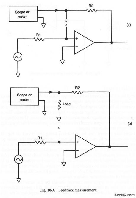
Because op-amp circuits usually include feedback, it is sometimes necessary to measure feedback voltage at a given frequency with given operating conditions.The basic feedback-measurement connections are shown in Fig. 10-A. Although it is possible to measure the feedback voltage, as shown in Fig. 10-Aa, a more accurate measurement is made when the feedback lead is terminated in the normal operating impedance(Fig.10-Ba).If an input resistance is used In thecircuit,and this resistance is considerably lower than the IC inputimpedance,usethe resistance value.If In doubt, measure the input impedance of the IC(asdescribed In chapter 1). Then,terminate the feedback lead In that value(tomeasure open-loop feedback voltage). Remember that open-loop voltage gammust be substantially higher than the closed-loop voltage gam for most Op-ampcircuits to perform properly. (View)
View full Circuit Diagram | Comments | Reading(542)
| Pages:128/195 At 20121122123124125126127128129130131132133134135136137138139140Under 20 |
Circuit Categories
power supply circuit
Amplifier Circuit
Basic Circuit
LED and Light Circuit
Sensor Circuit
Signal Processing
Electrical Equipment Circuit
Control Circuit
Remote Control Circuit
A/D-D/A Converter Circuit
Audio Circuit
Measuring and Test Circuit
Communication Circuit
Computer-Related Circuit
555 Circuit
Automotive Circuit
Repairing Circuit