
Signal Processing
Index 126
ac_coupled_comparator
Published:2009/7/24 4:24:00 Author:Jessie

Fig. 15-10 This circuit also buffers the input of an LM106 with an L102 voltage follower. The LM106 draws an input current that is twice the specified bias current when the signal is above the comparison threshold. This asymmetrical current drain charges a coupling capacitor that is connected directly to the LM106 input and it can produce an error. The problem is eliminated with a buffer because the input current to the LM106 is both low and constant. National Semiconductor. Linear Applications Handbook 1991 p. 1190. (View)
View full Circuit Diagram | Comments | Reading(917)
Zero_crossing_detector_with_low_input_current
Published:2009/7/24 4:23:00 Author:Jessie

Fig. 15-9 This circuit buffers the input of an LM106 with an LM102 voltage follower. Such an arrangement reduces effective input current of the LM106 comparator by more than three orders of magnitude without greatly reducing speed. The high input currents of many comparators result in reduced speed when used with high source resistances. If the input signal can exceed the common-mode range of the comparator (±5 V for the LM106), clamp diodes must be used as shown. It is then necessary to isolate the comparator from the input with a relatively large resistance to prevent loading. National semiconductor Linear Applications Handbook,1991,p. 1190. (View)
View full Circuit Diagram | Comments | Reading(937)
Simple_level_detector_using_a_comparator
Published:2009/7/24 4:27:00 Author:Jessie

Fig. 15-13 This circuit shows how a high-speed comparator (LM160) can be used as a level detector or line receiver. The hysteresis graph and equations show the relationship between input and output voltages.National Semiconductor Linear Applications Handbook. 1991. p. 326. (View)
View full Circuit Diagram | Comments | Reading(729)
Simple_zero_crossing_detector
Published:2009/7/24 4:32:00 Author:Jessie

Fig. 15-17 This circuit uses an LM108 op amp as a voltage comparator to produce a simple zero-crossing detector. The output is clamped so that the circuit can drive DTL or TTL directly. National Semiconductor Linea Applications Handbook 1991, p. 71. (View)
View full Circuit Diagram | Comments | Reading(1867)
Using_a_timer_as_a_comparator
Published:2009/7/24 4:31:00 Author:Jessie

Fig. 15-16 This circuit uses an LM122 timer as a comparator with adjustable threshold levels. The output can be inverted or noninverted, as selected by a switch (or permanent wiring). Using the values shown and a +5-V supply, the threshold can be set between 0 and 3 V. National Semiconductor, Linear Applications Handbook, 1991, p. 335. (View)
View full Circuit Diagram | Comments | Reading(605)
Comparing_voltages_of_opposite_polarity
Published:2009/7/24 4:40:00 Author:Jessie

Fig. 15-22 This circuit compares the magnitude of VIN1 and VIN2, which have opposite polarities. The voltage at the inverting input of the LM139 is a function of VIN1, VIN2, R1, and R2. Diode-connected Q1 clamps the inverting terminal below ground for protection. If VIN1 is used for positive and VIN2 for negative, the output goes low (ground) if VIN1 is greater than VIN2. The output goes to near VCC if VIN1 is less than VIN2 National Semiconductor. Linear Applications Handbook, 1991, p. 260. (View)
View full Circuit Diagram | Comments | Reading(618)
Fully_isolated_limit_comparator
Published:2009/7/24 4:36:00 Author:Jessie

Fig. 15-20 This circuit produces a digital output if the input is above or below a preset limit, and is ideal for process-control applications where transducers operate at high common-mode voltage, or where large loops exist. Amplifier C1 permits use of thermocouples and other low-level sources. The circuit functions by echoing an interrogation pulse if the input is above a preset level. If the input is below the leve1 (determined by the 1-MΩ level set), no echo occurs. Maximum common-mode voltage is limited by the transformers 500-V breakdown. Linear Technology, Linear Applications Handbook 1990, p. AN11-10. (View)
View full Circuit Diagram | Comments | Reading(452)
Complete_FM_IF_system_for_high_quality_receivers
Published:2009/7/24 4:35:00 Author:Jessie


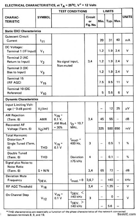
The CA3189 shown in this circuit includes an IF amplifier quadrature detector, AF preamplifier, and specific circuits for AGC, AFC, tuning meter, deviation-noise muting, and on-channel detector, as shown in Fig. 2-61B. Sensitivity is 12μV (typical) at -3-dB point. Typical characteristics are shown in Fig.2-61C (View)
View full Circuit Diagram | Comments | Reading(1678)
Micropower_comparator_with_high_current_switch
Published:2009/7/24 4:35:00 Author:Jessie

Fig. 15-19 This circuit provides a method of continuously monitoring an input voltage while dissipating only 100μW of power, but still being capable of switching a 500 mA load if the input exceeds a given value. The reference voltage can be any value between +8.5 and -8.5 V. The comparator resolves input voltage differences down into the 0.2-mV region. R1 provides for input-offset null. The load can be a resistor, relay coil, or lamp, so long as load current does not exceed 500 mA. For V+ less than 15 V and IL less than 25 mA, Q2 and R2 can be omitted. National Semiconductor Lineal Applications Handbook 1901, p. 205. (View)
View full Circuit Diagram | Comments | Reading(559)
Comparator_with_output_buffer
Published:2009/7/24 4:34:00 Author:Jessie


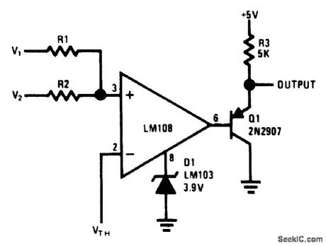
Fig, 15-18 This circuit uses an LM108 op amp as a comparator for voltages opposite polarity. The output changes state when the voltage on the junction R1/R2 is equal to VTH (at pin 2). This is expressed by:
National Semiconductor, Linear Applications Handbook, 1991, p. 71.
(View)
View full Circuit Diagram | Comments | Reading(673)
Opposite_polarity_magnitude_comparator
Published:2009/7/24 4:47:00 Author:Jessie

Pig. 15-28 This circuit is similar to that of Fig. 15-22, but it uses only one section of an LP165/365 and it requires a single supply. Figures 15-24B and 15-24C show the pin connections and electrical characteristics, respectively. Raytheon Linear Integrated circuits 1989, p. 5-40. (View)
View full Circuit Diagram | Comments | Reading(611)
Comparator_with_emitter_hysteresis
Published:2009/7/24 4:46:00 Author:Jessie

Fig. 15-27 This circuit shows an LP165/365 connected to improve hysteresis (using emitter positive feedback). Notice that this can only be used with one section of the quad LP165/365. Figures 15-24B and 15-24C show the pin connections and electrical characteristics, respectively. Raytheon Linear Integrated circuits 1989 p 5-40. (View)
View full Circuit Diagram | Comments | Reading(657)
Comparator_with_standard_hysteresis
Published:2009/7/24 4:45:00 Author:Jessie

Fig. 15-26 This circuit shows an LP165/365 connected to improve hysteresis (using the standard positive feedback). Figures 15-24B and 15-25C show the pin connections, and electrical characteristics, respectively. Raytheon Linear Integrated Circuits, 1989, p. 5-40. (View)
View full Circuit Diagram | Comments | Reading(629)
12_ns_circuit_breaker_using_a_comparator
Published:2009/7/24 4:41:00 Author:Jessie
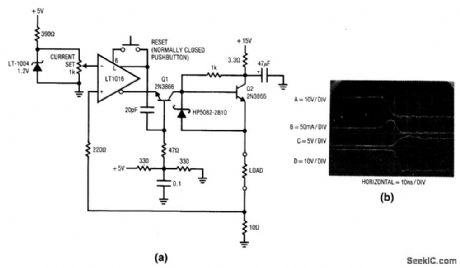
Fig. 15-23 This circuit uses a high-speed comparator (LT1016) to turn off current in a load 12 ns after the load exceeds a preset value. The circuit has been used to protect ICs during development and for protecting expensive loads during calibration. Under normal conditions, the voltage across the 10-Ω shunt is smaller than the potential at the LT1016 inverting input. This keeps Q1 off and Q2 receives bias, which drives the load, When an overload occurs (in this case via a test circuit, trace A, Fig. 15-23B) the current through the 10-Ω sense resistor begins to increase (trace B). When current exceeds the preset value, the LT1016 outputs reverse (the noninverting output is shown in trace C). This provides turn-on drive for Q1 and cuts Q2 off (Q2 emitter is trace D) in 5 ns. The delay from the onset of excessive load current to complete shutdown is 12 to 13 ns. Once the circuit is triggered, the LT1016 is held in the latched state by feedback from the noninverting output. When the load fault is cleared, the pushbutton can be used to reset the circuit. Linear Technology Linear Applications Handbook :990 p. AN13-24. (View)
View full Circuit Diagram | Comments | Reading(531)
Comparator_oscillator_clock_generator
Published:2009/7/24 4:56:00 Author:Jessie

Fig, 15-36 This self-starting fixed-frequency oscillator gives excellent frequency stability. The frequency is determined by R1/C1, and R2 provides the regenerative feedback. D1 enhances the stability by compensating for the difference between VOH and VSUPPLY. In applications where a precision clock generator up to 100 kHz is required, such as in automatic test equipment, C1 can be replaced by a crystal. Figures 15-32B and 15-32C show the pin connections and electrical characteristics, respectively. Harris Semiconductor. Linear & Telecom ICs, 1991, p. 4-30. (View)
View full Circuit Diagram | Comments | Reading(612)
Comparator_RS232_to_CMOS_line_receiver
Published:2009/7/24 4:54:00 Author:Jessie

Fig. 15-34 This RS232-type line receiver to drive CMOS logic uses a Schmitt-trigger feedback network to provide about 1-V input hysteresis for added noise immunity. The diodes and input resistor minimize transient spikes when the interface connection is made or broken. Figures 15-32B and 15-32C show the pin connections and electrical characteristics, respectively. Harris Semiconductor, Linear & Telecom ICs 1991, p. 4-30. (View)
View full Circuit Diagram | Comments | Reading(600)
EMITTER_COUPLED_RC_OSCILLATOR
Published:2009/7/1 2:34:00 Author:May

The circuit covers 15 Hz-30 kHz and is useful as a function generator. The 2N2926 or equivalent transistors can be used. (View)
View full Circuit Diagram | Comments | Reading(720)
Comparator_Schmitt_trigger
Published:2009/7/24 4:56:00 Author:Jessie

Fig. 15-37 This circuit is essentially a zero-crossing detector with hysteresis. The circuit has a 100-mV hysteresis, which can be used in applications, where very fast transition times are required at the output-even though the input signal is very slow. The hysteresis loop also reduces false triggering because of noise on the input. The waveforms in Fig. 15-37B show the trip points developed by the hysteresis loop. Figures 15-32B and 15-32C show the pin connections, and electrical characteristics, respectively. Harris semiconductor, Linear & Telecom ICs. 1991. p. 4-30. (View)
View full Circuit Diagram | Comments | Reading(1647)
LINEAR_TRIANGLE_SQUARE_WAVE_VCO
Published:2009/7/1 2:13:00 Author:May

The VCO has two buffered outputs; a triangle wave and a square wave. Frequency is dependent on the output voltage swing of the Schmitt trigger, IC2. Superior performance can be obtained by replacing Q1 with a switching FET. Fast FET op amps will improve high frequency performance. (View)
View full Circuit Diagram | Comments | Reading(3701)
QUAD_op_AMP_GENERATES_FOUR_DIFFERENT_SYNCHRONIZED_WAVEFORMS_SIMULTANEOUSLY
Published:2009/7/1 2:03:00 Author:May

A quad op amp can simultaneously generate four synchronized waveforms. The two comparators (A1 and A3) produce square and pulse waves, while the two integrators (A2 and A4) give triangular and sawtooth waves. Resistor R1 sets the duty cycle and the frequency, along with resistors R and capacitors C. (View)
View full Circuit Diagram | Comments | Reading(1180)
| Pages:126/195 At 20121122123124125126127128129130131132133134135136137138139140Under 20 |
Circuit Categories
power supply circuit
Amplifier Circuit
Basic Circuit
LED and Light Circuit
Sensor Circuit
Signal Processing
Electrical Equipment Circuit
Control Circuit
Remote Control Circuit
A/D-D/A Converter Circuit
Audio Circuit
Measuring and Test Circuit
Communication Circuit
Computer-Related Circuit
555 Circuit
Automotive Circuit
Repairing Circuit