
Signal Processing
Index 138
SINE_WAVE_OSCILLATOR
Published:2009/6/24 2:31:00 Author:May

The oscillator delivers a high-purity sinusoid with a stable frequency and amplitude. (View)
View full Circuit Diagram | Comments | Reading(0)
AUDIO_OSCILLATOR
Published:2009/6/24 2:30:00 Author:May

Almost any transistor will work. R1 and C1 will vary the tone. (View)
View full Circuit Diagram | Comments | Reading(0)
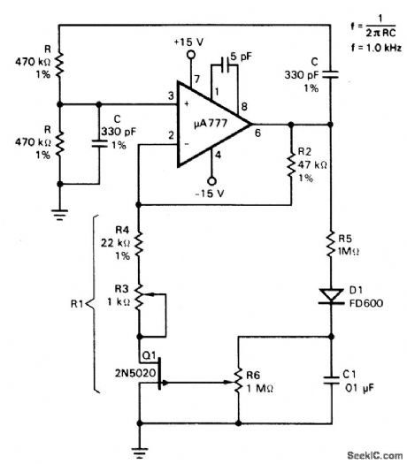
VERY_LOW_FREOUENCY_GENERATOR
Published:2009/6/24 2:29:00 Author:May

Wien bridge oscillator generates frequen-cies of 1 Hz and 2 to 20 Hz in 2 Hz steps. Maximum output amplitude is 3 volts rms of8.5 volts peak-to-peak. A pot-and-switch at-tenuator allows the output level to be set with a fair degree of precision to any value within a range of 5 decades. (View)
View full Circuit Diagram | Comments | Reading(1073)
WIEN_BRIDGE_OSCILLATOR_2
Published:2009/6/24 2:27:00 Author:May

View full Circuit Diagram | Comments | Reading(531)
WIEN_BRIDGE_OSCILLATOR_1
Published:2009/6/24 2:26:00 Author:May

Wien bridge sine-wave oscillator using two RCA CA3140 op amps covers 30 Hz to 100 kHz with less than 0.5 percent total harmonic distortion. The 10k pot is adjusted for the best waveform. Capacitor C1 and C2 are a two-gang, 450-pF variable with its frame isolated from ground. Maximum output into a 600-ohm load is about 1 volt rms. (View)
View full Circuit Diagram | Comments | Reading(1382)
WIEN_BRIDGE_OSCILLATOR
Published:2009/6/24 2:24:00 Author:May
Field effect transistor, Q1, operates in the linear resistive region to provide automatic gain control. Because the attenuation of the RC network is one-third at the zero phase-shift oscillation frequency, the amplifier gain de-termined by resistor R2 and equivalent resis-tor RI must be just equal to three to make up the unity gain positive feedback requirement needed for stable oscillation. Resistors R3 and R4 are set to approximately 1000 ohm less than the required RI resistance. The FET dynami-cally provides the trimming resistance needed to make RI one-half of the resistance of R2. The circuit composed of R5, D1, and C1 iso-lates, rectifies, and filters the output sine wave, converting it into a dc potential to con-trol the gate of the FET. For the low drain-to-source voltages used, the FET provides a symmetrical linear resistance for a given gate-to-source voltage. (View)
View full Circuit Diagram | Comments | Reading(0)
NOISE_GENERATOR
Published:2009/6/24 2:04:00 Author:May

This circuit generates noise pulses that are suitable for test purposes, etc. A zener diode is used as a noise source. IC1 is a relaxation oscillator. P1 determines noise bandwidth, and P2 and P3 the noise amplification. Current consumption is 10 mA @ 12 Vdc. (View)
View full Circuit Diagram | Comments | Reading(4)
TOP_OCTAVE_GENERATOR
Published:2009/6/24 1:59:00 Author:May
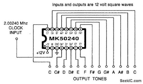
Using an MK50240, this circuit produces 12 top octave tones. The input and output lines can be divided using a binary divider IC to obtain the lower notes. (View)
View full Circuit Diagram | Comments | Reading(1484)
Low frequency signal generator(2Hz,4Hz,60Hz,120Hz)
Published:2011/7/29 2:26:00 Author:Ecco | Keyword: Low frequency, signal generator, 2Hz, 4Hz, 60Hz, 120Hz

Low frequency signal generator can be used to measure the sensitivity of amplifier, frequency response, frequency compensation, tone control, it is very useful measuring instruments to repair low-frequency amplifier. It is also used as a digital clock source. Depending on the actual use, the signal generator outputs eight fixed frequencies, selecting switch arbitrarily, the voltage output range can be adjusted in two blocks of 0 ~ 0.1V, 0 ~ 1V. The working principle is shown as the chart. IC CD4060 is a fourteen divider with an oscillator. The crystal SJT produces a 30720Hz weak signal frequency, and it forms a crystal oscillator with Cl and the internal of CD4060 inverter. Rl is used to provide feedback loop, it can only produce oscillation on the fundamental frequency of crystal, the oscillation center frequency is 30720Hz. The tuning capacitor Cl makes the frequency tune at the center frequency. SA is placed at pin 3 of CD4060. 30720Hz is divided by CD4060 nine stage(512 times), the pin 13 outputs high accuracy 60Hz output frequency, the capacitor C3 coupled it to the pin 2 of 741 op-amp for signal amplification, then outputed form pin 6 of 741.
(View)
View full Circuit Diagram | Comments | Reading(2937)
56 ~ 484 khz high frequency oscillator
Published:2011/7/29 1:56:00 Author:Ecco | Keyword: 56 ~ 484 khz high frequency oscillator
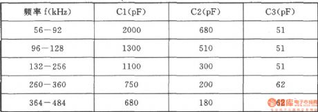
High frequency oscillator is shown as the figure, it can be used as special high-frequency generator, selecting different capacitance between 56 ~ 484 kHz can generate a high frequency. The circuit has the advantages of good shave waveform, high stability of frequency, low output impedance. Selection of components: transistor VTl, VT2: 3DG6D, 65 ≤ β 115, VT3, VT4: 3DGl308, 60 ≤ β ≤ 85. Semi-adjustable capacitor C4: CCWX-3-5/20pF. Crystal SJT: BE-42 type. K: JZX-10M (mini relay). Light-emitting diode VD4: BT-605 (red, green color). Variable device T: using MXD-2000 ferrite, GV-30 × 19 core. Ll-2Φ0.21mm high-strength wire with 133-turn winding, L3-4Φ0.21mm high-strength wire with 11 turns, L5-6Φ0.21mm high-strength wire with 80 turns. Nominal power of resistor uses l/2WRJ models and R27, the other type of resistor are 1/8WRJ. Other parameters of marked element are shown as the chart, there’s no special requirement. The relationship between frequency and capacitor values are shown as below.
(View)
View full Circuit Diagram | Comments | Reading(805)
48MHz HCMOS Oscillator
Published:2011/7/29 2:03:00 Author:Ecco | Keyword: 48MHz, HCMOS, Oscillator
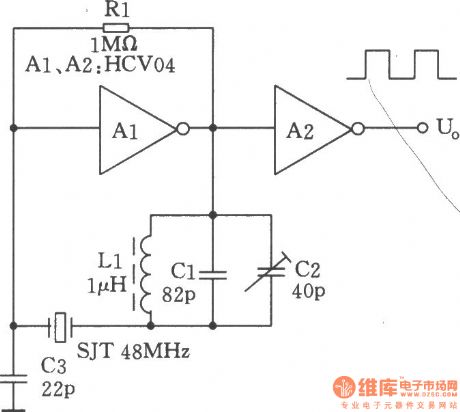
The figure shows the 48MHzcrystal oscillator composed of HCMOS IC. The fundamental frequency of the crystal is l6MHz, butit works in the third harmonic oscillator by force. Harmonic oscillator suppresses the fundamental frequency of the crystal, the parallel resonant circuit in the figure resonances on the base frequenciesof crystal. Connecting to crystal SJT in series may have the highest impedance to fundamental frequency, which can effectively inhibit the fundamental frequency oscillations andensure the third harmonic being easy to start up.
(View)
View full Circuit Diagram | Comments | Reading(1361)
The sine wave oscillator circuit with adjustable frequency, constant amplitude composed of F007
Published:2011/7/29 2:09:00 Author:Ecco | Keyword: sine wave oscillator , adjustable frequency, constant amplitude


Figure shows the sine wave oscillator circuit with adjustable frequency, constant amplitude. The circuit consists of two sub-phase circuit and a linear concatenation of the inverting amplifier. Phase-shifting circuit is the combination of integrated operational amplifier A1, A2 and the RC. Since the phase shift of inverter A3 is 180o, therefore, two phase circuits should also be phase-shifted 180o to ensure that the requirements of the circuit oscillation condition with the total phase shift in 360o.The dynamic resistance of diodes D1, D2 is very high when the voltage being low, so the high-gain inverting circuit ensures the start-up circuit. When the oscillation amplitude rises, the dynamic resistance of D1, D2 getting smaller and smaller reduce the gain of the circuit, so that the output amplitude is stable. Because the diode has a larger dead zone voltage, small signal output waveform has stopped, it is added a resistor R2. The oscillation frequency of the circuit:
Adjusting potentiometer W1 and W2 can change the frequency. As the phase shift circuit has no effect on amplitude, the regulation frequency does not affect the stability of amplitude. W1 can adjust the frequency changing in about 10 times, the scope of its regulatory role is not obvious when over the range, then it can be adjusted by w2.
(View)
View full Circuit Diagram | Comments | Reading(2232)
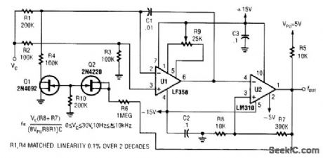
Wideband sine wave VCO composed of LF356N
Published:2011/7/29 2:10:00 Author:Ecco | Keyword: Wideband , sine wave, VCO
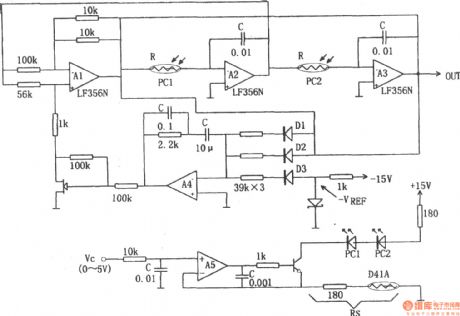
The chart shows the wideband sine wave VCO. Oscillation frequency of the circuit is decided by the resistor R and capacitor C , andthe applied voltage Vc and controlling resistor R constitute theVCO. Variable resistor in the circuit uses photo coupler PC1 and PC2, the rectifier circuit adopts average detection mode. The actual operating frequency of the circuit is tens of Hz or more. In addition, the characteristics of the control voltage Vc with respect to the oscillation frequency depends on the characteristics of optocouplers. The light source of optocoupler is LED and it needs current driving, so the circuit uses the constant current source circuit composed of 4559 operational amplifier. Voltage / current conversion uses Rs, Rs can choose the maximum control voltage Vc freely. In the circuit, IFmax = 30mA, Vcmax = 5V, resistor Rs = 180Ω.
(View)
View full Circuit Diagram | Comments | Reading(1917)
1.8 kHz signal generator
Published:2011/7/29 2:27:00 Author:Ecco | Keyword: 1.8 kHz , signal generator
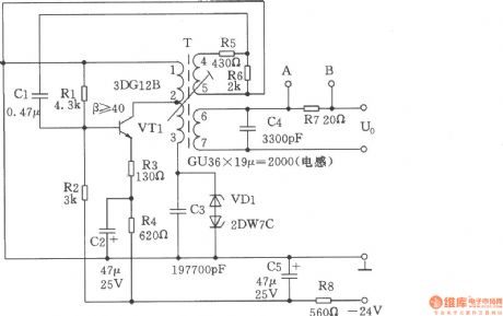
The circuit is shown as the chart, it selects the best working conditions and reasonable temperature coefficient of components in resonant circuit. It also takes Ac regulator measures both ends of the resonance in order to obtain a good output amplitude and frequency stability. Temperature is +25 ℃ ± 20 ℃. The supply voltage changes in the range -40% of -24V, frequency: △ f ≤ 2Hz, the output level: △ dB ≤ 0.26dB.
(View)
View full Circuit Diagram | Comments | Reading(496)
800Hz signal generator
Published:2011/7/29 2:27:00 Author:Ecco | Keyword: 800Hz , signal generator
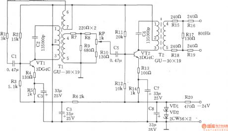
It is a LC oscillator circuit with800Hz oscillation level for the transformer coupled, it's a simple circuit, the frequency is stable. Buffer amplifier isused for reducing distortion, it can adjust the output level by potentiometer. 1. Specifications (1) operating frequency: 800Hz; (2) Frequency stability: ≤ ± 20Hz; (3) Output Level: 0dB/600Ω. 2.Working principle of the circuit is shown as the circuit. 800Hz signal generator is composed of LC oscillator and buffer amplifier. Oscillator: tuned transformer Tl is used as LC oscillation tank and output transformer, C2 is the tuned capacitor. The inductance of oscillation tank is the positive temperature coefficient, and polystyrene capacitor is the negative temperature coefficient, so the compensation of temperature coefficient improve the frequency stability. R2, R3 are DC bias resistors. R4, R5 are the emitter resistors of VTl, R4 has a current negative feedback. C3 is a bypass capacitor R5. R6 and R4 form a decoupling circuit for inter-stage power supply, R7, R8, R9 form the buffer attenuation device; buffer amplifier stage: C5 is the coupling capacitor, R11, Rl2 are bias resistors of VT2, Rl3, Rl4 are the emitter resistors of VT2, C7 is bypass capacitor of R14, C6 and T2 form a tuned output circuit to reduce distortion, RP potentiometer is used to adjust the output level. Buffer amplifier output terminal connecting to a 600Ω attenuation with Rl5 ~ Rl9 could provide 0dB output level. VDl, VD2, R20, C8 constitute regulator circuit.
(View)
View full Circuit Diagram | Comments | Reading(637)
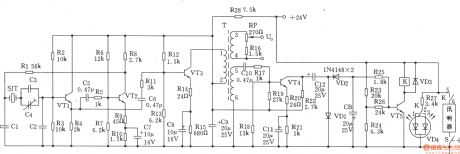
12kHz IF oscillator
Published:2011/7/29 2:36:00 Author:Ecco | Keyword: 12kHz , IF , oscillator
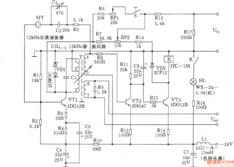
The 12kHz oscillator shown as the chart is composed of 12kHz crystal oscillator, output level adjustment circuit, level rising circuit and the alarm circuit. It employs a novel single-tube tuner variable feedback control oscillation circuit, and in the feedback loop, it connects a 12kHz quartz crystal resonator in series, so that the oscillation frequency depends on the the performance of l2kHz quartz crystal resonators. For improving the reliability and output of the oscillator amplitude stability, it uses AC stable exchange rate circuit, in other respects, the circuit uses the devices with high performance and reliability to obtain excellent performance. Technical characteristics: (1) Nominal frequency: 12kHz; (2) Frequency Accuracy: △ f ≤ ± 0.5Hz; (3) Frequency stability: the temperature is 25 ℃ ± 20 ℃ range, △ f ≤ ± lHz ; (4) output level U01: -40.8dB/600Ω, align the scope: ≥ 3.5dB. Level stability △ dB ≤ ± 0.17dB. When the switch S is closed, U01 level enhances l0.5dB; (5) output level U02: +3.5 ± 0.8dB/1.2kΩ; (6) When the oscillator stops oscillation, there is visible alarm signal.
(View)
View full Circuit Diagram | Comments | Reading(649)
12kHz intermediate frequency signal generator
Published:2011/7/29 1:52:00 Author:Ecco | Keyword: 12kHz, intermediate frequency , signal generator
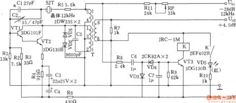
The circuit shown as the chart is composed of l2kHz intermediate-frequency oscillator and alarm circuit. It uses the variable feedback oscillation circuit, and its frequency is determined mainly by the quartz crystal. Cl, C2 can be used for fine tuning frequency. The oscillating tube adopts multiple-unit tube to increase the input impedance, the stability of magnitude could be gotten by bi-directional regulated voltage of VDl and VD2. Specifications: (1) Nominal frequency: 12kHz, the frequency difference does not exceed ± 1Hz; (2) Frequency Accuracy: In the temperature range of 25 ± 25 ℃, ΔF does not exceed ± lHz; (3) U01 output level: -28dB/600Ω, deviation is less than ± 0.2dB; (4) U02 output level: +4.5 dB ± 0.5dB. (View)
View full Circuit Diagram | Comments | Reading(706)
SINUSOIDAL_3_Hz_TO_300_kHz_VCO
Published:2009/6/23 4:15:00 Author:May
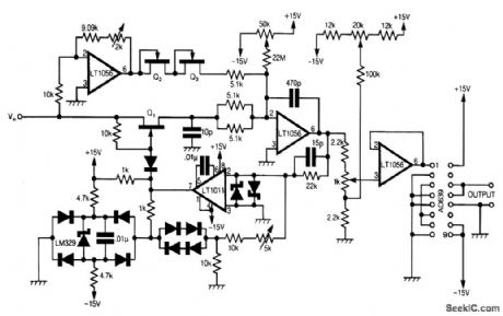


This circuit uses Analog Devices' AD639 universal trigonometric function generator to convert a triangle waveform, the basic waveform of the VCO itself, into a very low-distortion sine wave.By using the AD639 in its frequency tripler mode [2], the frequency range 3 Hz to 300 kHz is now covered. The circuit has been drawn here so that the oscillator loop, consisting of Q1, the integrator and the LT1011 comparator, is clearly shown.When Q1 is off, the input amplifier, which is adjusted to have a gain of exactly -1, pulls a current VIN/R, where R is 5.1 kΩ in series with two JFETs, and Q2 and Q3, out of the virtual earth of the in-tegrator. The output of the integrator thus rises at a rate of VIN/CR, where C = 470 pF. At a level that can be adjusted by the 5-kΩ potentiometer, the comparator flips and turns on Q1.A current of exactly 2VIN/R, is now supplied to the virtual earth of the integrator because there are now two 5.1-kΩ resistors in parallel and only a single JFET in between the virtual earth and Vin.The integrator output now falls at a rate of VIN/CR and the cycle repeats. Any offset in the current to the virtual earth of the integrator, due to circuit board leakage, etc., can be corrected by adjusting the 50-kΩ potentiometer. It follows that the symmetry of the triangle wave at the integrator output can be corrected by adjusting the 2-kΩ potentiometer, and the 50-kΩ potentiometer at VLF, and the frequency can be trimmed with the 5-kΩ potentiometer.The l-kΩ potentiometer variable is adjusted to give the input level to the AD639 needed to drive it over ±270°and so produce a sinusoidal output at three times the frequency of the triangle-wave input. Offset correction for the AD639 is made at the input to the voltage follower by means of the 20-kΩ potentiometer.Once a symmetric triangle wave has been obtained by adjusting the 2-kΩ and 50-kΩ poten-tiometers, and the correct frequency of 100 kHz has been set for VIN/=10 V, by adjusting the 5-kΩ potentiometer, the triple-frequency she-wave output can be set up by adjustment of the 1-kΩ and 20-kΩ potentiometers.This is best done by triggering the CRO from the triangle wave, and then viewing at least three complete cycles of output. Having adjusted for a clean-looking sine wave, the final adjustment of the 1-kΩ and 20-kΩ potentiometers should be made on a single sinusoidal cycle display, using internal trigger so that the three slightly different parts of the output cycle lie one upon the other and can be made to merge. Q1, Q2, and Q3 are 2N4391s, the two Schottlqr diodes are 5082-2810, and the other nine diodes are 1N914.All device power supply pins should be decoupled with 0.33 p.F. Resistors associated with the in-puts of the devices should be 1% high-stability parts. (View)
View full Circuit Diagram | Comments | Reading(2973)
SIMPLE_VIDEO_LINE_BAR_GENERATOR
Published:2009/6/23 4:02:00 Author:May
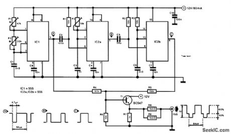
A 555 and a dual 556 timer generate a rudimentary video signal, as shown in the schematic. The first timer generates 4.7-μs synch pulses operating in the astable mode with a 64-μs period. The sec-ond timer generates a delay pulse, which triggers the third timer to generate a bar. The second timer sets the bar position and the third sets the bar width. (View)
View full Circuit Diagram | Comments | Reading(2211)
10_Hz_TO_10_kHz_3_DECADE_VCO
Published:2009/6/23 4:37:00 Author:May
View full Circuit Diagram | Comments | Reading(0)
| Pages:138/195 At 20121122123124125126127128129130131132133134135136137138139140Under 20 |
Circuit Categories
power supply circuit
Amplifier Circuit
Basic Circuit
LED and Light Circuit
Sensor Circuit
Signal Processing
Electrical Equipment Circuit
Control Circuit
Remote Control Circuit
A/D-D/A Converter Circuit
Audio Circuit
Measuring and Test Circuit
Communication Circuit
Computer-Related Circuit
555 Circuit
Automotive Circuit
Repairing Circuit