
Circuit Diagram
Index 1737
The door control lamp circuit (with the electric timer and alarm)
Published:2011/6/21 22:30:00 Author:qqtang | Keyword: door control lamp, electric timer
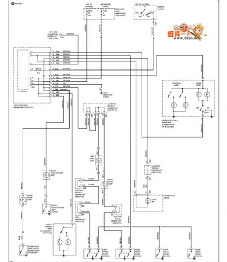
The door control lamp circuit (with the electric timer and alarm) is shown as above.
(View)
View full Circuit Diagram | Comments | Reading(939)
The general power supply loading circuit with the usage of bulbs
Published:2011/6/21 22:28:00 Author:qqtang | Keyword: power supply, bulb

View full Circuit Diagram | Comments | Reading(752)
The analytical circuit of the multi-function remote alarm controller
Published:2011/6/21 22:41:00 Author:qqtang | Keyword: analytical circuit, multi-function, remote
View full Circuit Diagram | Comments | Reading(495)
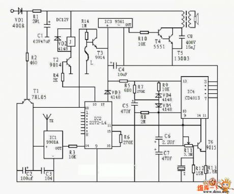
The key ring wireless encoding remote control circuit (1)
Published:2011/6/21 22:32:00 Author:qqtang | Keyword: key ring, remote control
View full Circuit Diagram | Comments | Reading(622)
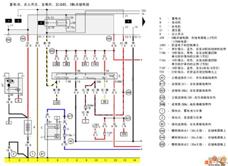
The Shanghai Passat basic circuit
Published:2011/6/19 20:40:00 Author:qqtang | Keyword: Passat, basic circuit
The flash mode connection circuit is shown in the figure.
(View)
View full Circuit Diagram | Comments | Reading(492)
The adv7175 and adv7176 digital video encoding integrated video amplifier circuit
Published:2011/6/19 20:46:00 Author:qqtang | Keyword: video encoding, integrated video amplifier

The adv7175 and adv7176 digital video encoding integrated video amplifier circuit in shown in the figure.
(View)
View full Circuit Diagram | Comments | Reading(738)
Operational Amplifier Absorber Circuit
Published:2011/6/14 23:35:00 Author:Robert | Keyword: Operational Amplifier, Absorber


The operational amplifier is a device with high gain. By adding deep negative feedback when using, the operational amplifier can get good closed loop characteristic. But the negative feedback circuit always bring phaseshift for high-frequency signals. When this phaseshift get to 180。it would make the negative feedback to be positive feedback, so it would generate parasitic self-oscillation to make the opertaional amplifier unable to work normally. In the low frequency the self-oscillation is mostly generated by common power coupling. This case can be solved by strengthening the decoupling. In the high frequency the self-oscillation is solved by corresponding phase compensation method. (View)
View full Circuit Diagram | Comments | Reading(591)
CGO602CESA Single-Chip Remote Control Transmitter Integrated Circuit
Published:2011/6/14 23:35:00 Author:Robert | Keyword: Single-Chip, Remote Control, Transmitter, Integrated


The CGO602CESA is a single-chip remote control transmitter integrated circuit which can be used in many kinds of remote control systems such as TV set, audio device, player and so on. The CGO602CESA integrated circuit has internal remote control telecommand encoder, keys scanning pulses generater, clock oscillation circuit, emission signal buffer, testing circuit and other some accessory circuit. The CGO602CESA integrated circuit uses 36 feet quartet packaging, its foot function and data is shown in the table 1. The remote control transmitter's typical application circuit composed of CGO602CESA integrated circuit is shown in picture 1. (View)
View full Circuit Diagram | Comments | Reading(561)
Operational amplifier anti-blocking circuit
Published:2011/6/13 4:51:00 Author:Christina | Keyword: Operational amplifier, anti-blocking

If we add the large signal or the larger interference to the reverse phase input port of the operational amplifier, the amplifier always can't work normally, and there will be the phenomenon of the signal can not enter the amplifier or the output intermittent, at this time, you must turn off the power supply then turn on again or remove the signal for a period of time, so the amplifier can return to normal. This phenomenon called the blockade or the lockout. This phenomenon is caused by: the transistor of the input stage is saturated, the reverse phase input port and output port lose the nature of the opposite phase, so the circuit changes into the positive feedback.
(View)
View full Circuit Diagram | Comments | Reading(624)
CEC910 fan single chip microcomputer integrated circuit
Published:2011/6/13 4:56:00 Author:Christina | Keyword: fan, single chip, microcomputer, integrated circuit
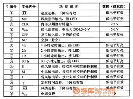
The CEC910 is designed as one kind of fan single chip microcomputer integrated circuit, and it can be used in the speed regulation or the power regulation applications of the fan and all sorts of small home appliances.
The CEC910 is in the 16-pin dual-row DIP plastic package, the pin functions and data is as shown in the table 1, the typical application circuit is as shown in figure 1.
Table 1 The pin functions and data of the CEC910
Figure 1 The typical application circuit of the CEC910
(View)
View full Circuit Diagram | Comments | Reading(591)
Operational amplifier zero adjustment circuit
Published:2011/6/13 5:14:00 Author:Christina | Keyword: Operational amplifier, zero adjustment


The common zero adjustment circuit is as shown in the figure.
The operational amplifier zero adjustment circuit
In figure (a), the potentiometer RP is connected with the internal input differential amplifier stage to change the voltage difference of the collector electrode, by this method, you can adjust the zero point; or you can connect the potentiometer RP2 with the input port of the integrated operational amplifier, let the bias current flow through the RP2 to cause the imbalance of the two input bias currents, so you can adjust the zero point.
For some pperational amplifiers with low drift and small input current, you can add a high resistance potentiometer to the collector electrode of the input amplifier stage according to the polarity of the partial zero to make the collector resistance imbalance to change the electric potential difference of the input stage, so the output is zero, as the figure (b) shows.
The auxiliaryzero adjustmentcircuit (View)
View full Circuit Diagram | Comments | Reading(1582)
CD4069 six NOT gates integrated circuit
Published:2011/6/13 6:16:00 Author:Christina | Keyword: six NOT gates, integrated circuit


The CD4069 is designed as one kind of CMOS general six NOT gates integrated circuit that can be used in wide range of applications, and it can be used to form the oscillator, buffer, trigger and inverter.etc.
1.The internal circuit block diagram
The CD4069 is in the 14-pin dual-row DIP package, the internal circuit block diagram is as shown in figure 1.
Figure 1 The internal circuit block diagram of the CD4069
2.The open resistance between the pins
The open resistance between the pins of the CD4069 which is measured by the 500 multimeter is as shown in figure 1.
Figure 1 The open resistance between the pins of the CD4069
PS: When you are measuring this resistance, you use the black pen to touch the pin, when the pin recovers the normal position, some times the resistance is 13KΩ, and if you disconnect the pen, the resistance is ∞. (View)
View full Circuit Diagram | Comments | Reading(1075)
CD4066 4-channel electronic switch integrated circuit
Published:2011/6/13 6:31:00 Author:Christina | Keyword: 4-channel, electronic switch, integrated circuit


The CD4066 is designed as one kind of 4-channel electronic switch integrated circuit that can be used in wide range of applications such as the TV, VCD, telephone and All kinds of electronic instrument meter.
1.Features
The CD4066 is mainly composed of four channels of electronic switch with the same functions, each electronic switch is controlled by the corresponding pin's input electrical level, the electrical level turns on or turns off the electronic switch. Their control pins are pin-13 (controls the pin-1 and pin-2), pin-5 (controls the pin-3 and pin-4), pin-6 (controls the pin-8 and pin-9), pin-12 (controls the pin-10 and pin-11).
2.Pin functions and data
The CD4066 is in the 14-pin dual-row DIP package, the pin functions and application measured data of the cordless telephone is as shown in table 1.
Table 1 The CD4066's pin functions and application measured data of the cordless telephone
3.The typical application circuit
The CD4066's typical application circuit of the cordless telephone is as shown in figure 1.
Figure 1 The CD4066's typical application circuit of the cordless telephone
(View)
View full Circuit Diagram | Comments | Reading(2294)
Feedback circuit
Published:2011/6/13 6:50:00 Author:Christina | Keyword: Feedback


In the practical applications, we usually need to add the feedback circuit to the operational amplifier. Because the open-loop gain of the operational amplifier is high, but in the practical applications the open-loop gain of the operational amplifier is not high, so we need to add the negative feedback circuit to form the closed loop to get the corresponding functions. In addition, in the depth feedback conditions, the performance of the operational amplifier will be much better.
Same-phase input feedback amplifier circuit
The figure shows the same-phase input feedback amplifier circuit. We add the negative feedback resistance Rf from the output port to the reverse phase input, the input voltage is input from the same-phase port.
According to the open loop voltage gain expression, we can list:
Reverse phase input feedback amplifier circuit:
Closed-loop gain:
The negative sign of the formula means the phase position of the output voltage and the input voltage is opposite. The formula shows that as long as the AUD is large enough, the closed-loop gain of this amplifier is only decided by the ratio of the resistance Rf and resistance R1, it has nothing to do with other parameters. (View)
View full Circuit Diagram | Comments | Reading(803)
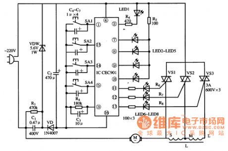
50Hz rectangular wave generator circuit
Published:2011/6/13 6:59:00 Author:Christina | Keyword: 50Hz, rectangular wave, generator
The figure shows the Schmidt shaping circuit that changes the sinusoidal voltage into the rectangular wave. The sinusoidal voltage which is reduced by the transformer adds to the base electrode of VT1 directly. In the positive half cycle of the alternating current, the diode VD conducts, the base electrode electric potential of VT1 is positive, so the VT1 cuts off, VT2 conducts. In the negative half cycle of the alternating current, the base electrode electric potential of VT1 is negative, VT1 conducts and the 5OHz rectangular wave is output by the collector electrode of VT2.
Figure The 50Hz rectangular wave generator circuit
(View)
View full Circuit Diagram | Comments | Reading(557)
27MHz crystal oscillator circuit
Published:2011/6/13 7:11:00 Author:Christina | Keyword: 27MHz, crystal oscillator

The 27MHz crystal oscillator circuit is as shown in the figure. The R1, R2, R3 are the biasing resistor, the C6 is the bypass capacitor, the voltage division circuit is composed of the C1, C3, C4 and C2 to control the oscillation strength. The L1 is the high-frequency choking coil which has the filtering effect.
The quartz crystal is in the parallel resonant state, the oscillation frequency of the oscillator depends on the natural frequency of quartz crystal. The L2 and C5 decide the oscillation strength.
Figure 15 The 27MHz crystal oscillator circuit
(View)
View full Circuit Diagram | Comments | Reading(4619)
Game-scoring Display Screen Circuit Diagram
Published:2011/6/16 10:58:00 Author:Vicky | Keyword: Game-scoring Display Screen

Game-scoring display screen circuit diagram is shown as in the above picture. The circuit is composed of add/subtract scoring input circuit, add/subtract scoring circuit, counting - decoding display circuit and reset circuit. (View)
View full Circuit Diagram | Comments | Reading(2049)
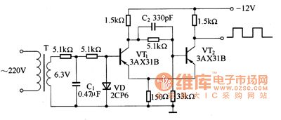
Unijunction Transistor (UJT) Work Performance Quick Test Circuit Diagram
Published:2011/6/18 10:21:00 Author:Vicky | Keyword: Unijunction Transistor (UJT) Performance Quick Test
The above picture is a circuit of unijunction transistor (UJT) work performance quick test .The tested unijunction transistor (UJT) VBT (suppose: BT33) constitutes relaxation oscillator together with R3 and C2. When the VBT is on, triode VT1 acquires bias current via bias resistance R2 (S1 is broke and S2 is closed up in the moment), and the luminous diode H1 gives out light. +10V power supply charges C2 via VD2 by R3. Voltmeter V can detect that the voltage of two ends of C2 would goes up continuously. When the electric potential of E end reaches the peak voltage, part from E to B1 of VBT would automatically breakover and the voltage of capacitance C1 would discharge via part from E to B1, both of which leads to emitter junction of triode VT1 ends because of back bias. (View)
View full Circuit Diagram | Comments | Reading(1968)
Quartz Crystal Selection Circuit Diagram
Published:2011/6/18 10:18:00 Author:Vicky | Keyword: Quartz Crystal Selection
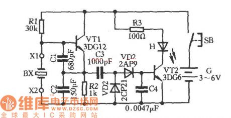
As shown in the above picture, BX is a Quartz Crystal (also called crystal oscillator) under test. Plug it into sockets X1 and X2, and press button SB. If BX is good, the oscillator composed of triode VT1, capacitances C1 and C2 works. The oscillator signal was sent from VT1 emitter, and coupled to VD2 via C3 to process detection and C4 filtering. It then becomes direct current and is sent to VT2 base electrode to make VT2 conducted and luminous diode H give out light, which is an indication that the quartz crystal is good. If H doesn’t give out light, then the quartz crystal is bad. By changing the capacitance value of C1 and C2 appropriately, it can be used to test quartz crystals of different frequency. (View)
View full Circuit Diagram | Comments | Reading(798)
OOK 315MHz Emitter Module Circuit Diagram
Published:2011/6/19 3:54:00 Author:Vicky | Keyword: OOK 315MHz Emitter Module

DKl000T is an emitter module composed by RF2516 and roll-code encoding device. Correspondingreceptor module is DKl000R. DKl000T is suitable to be applied in keyless-entering system, wireless safe system, remote monitoring and remote control.
Main technical features are listed as follows:
·Operating frequency: 315MHz;
·Modulation mode of 00K;
·Roll-code encoding;
·LED indicator;
·Output power: 70 dBμV/m 5;
·Voltage of power supply: 2~3 V ;
·Dissipation of current: 4~9 mA;
· Printing the antenna in the printing board.
Applied circuit of DKl000T module 315Hhz
(View)
View full Circuit Diagram | Comments | Reading(1303)
| Pages:1737/2234 At 2017211722172317241725172617271728172917301731173217331734173517361737173817391740Under 20 |
Circuit Categories
power supply circuit
Amplifier Circuit
Basic Circuit
LED and Light Circuit
Sensor Circuit
Signal Processing
Electrical Equipment Circuit
Control Circuit
Remote Control Circuit
A/D-D/A Converter Circuit
Audio Circuit
Measuring and Test Circuit
Communication Circuit
Computer-Related Circuit
555 Circuit
Automotive Circuit
Repairing Circuit