

About SeekIC | Services | Payment | Advertisements service | Contact Us | Links
© 2008-2012 SeekIC.com Corp.All Rights Reserved.

Published:2011/6/20 22:04:00 Author:Seven | Keyword: application circuit

The STK4172 application circuit is shown in the above figure.
(View)
View full Circuit Diagram | Comments | Reading(5422)
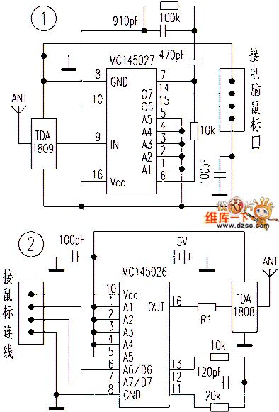
Published:2011/6/19 10:03:00 Author:Seven | Keyword: logic frame circuit
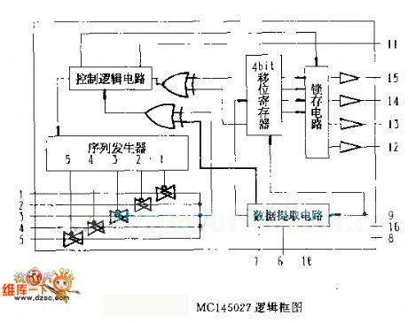
The MCl45027 logic frame circuit (View)
View full Circuit Diagram | Comments | Reading(397)
Published:2011/6/19 10:19:00 Author:Seven | Keyword: infrared, remote control
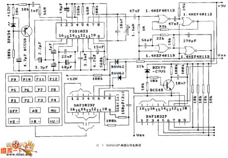
The SAFl032F typical application circuit (View)
View full Circuit Diagram | Comments | Reading(462)
Published:2011/6/19 10:22:00 Author:Seven | Keyword: drive circuit, discrete components

The IGBT drive circuit composed of discrete components
(View)
View full Circuit Diagram | Comments | Reading(4099)
Published:2011/6/21 22:23:00 Author:qqtang | Keyword: push-pull, switch power supply

The typical circuit of the push-pull switch power supply is shown in the figure, which belongs to the 2-terminal converting circuit, the magnetic core of the high-frequency transformer is working on the two sides of the hysteresis return. The circuit is installed with two switch pipes, VT1 and VT2, the two switches are conducting and blocked in turn under the control of the external motivating square wave signals, the square wave voltage is generated at the second coil of the transformer T, and then the voltage becomes a DC voltage after it is filtered.
The virtues of the circuit is that it's easy to drive with 2 switch pipes, and the main weakness is that the withstand voltage has to be the twice of the peak value of the circuit. (View)
View full Circuit Diagram | Comments | Reading(1515)
Published:2011/6/20 22:05:00 Author:Seven | Keyword: ultrasonic humidifier
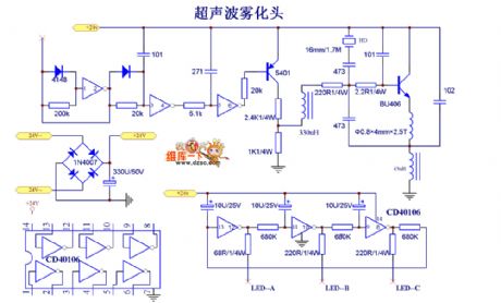
The ultrasonic humidifier circuit is shown in the above figure.
(View)
View full Circuit Diagram | Comments | Reading(6267)
Published:2011/6/19 10:25:00 Author:Seven | Keyword: fancy lamp
View full Circuit Diagram | Comments | Reading(615)
Published:2011/6/20 1:14:00 Author:Seven | Keyword: over-voltage, insulated gate, transistor grid

The reason of IGBT grid over-voltage:1. The static electricities assemble at the grid and cause over-voltage; 2. The capacitor Miller effect cause the grid over-voltage.
To prevent IGBT grid-emitter from being over-voltage, we should connect a several KΩ resistor between the grid and emitter of IGBT, see as the figure. The resistor should be close to the grid and the emitter. (View)
View full Circuit Diagram | Comments | Reading(663)
Published:2011/6/20 22:05:00 Author:Seven | Keyword: ultrasonic wave, remote control, working principle

The ultrasonic wave remote control lamp switch working principle and circuit (1) is shown as above:
(View)
View full Circuit Diagram | Comments | Reading(1502)
Published:2011/6/20 1:17:00 Author:Seven | Keyword: working principle, ultrasonic wave, remote control lamp
The working principle and circuit of the ultrasonic wave remote control lamp switchis shown in the figure.
(View)
View full Circuit Diagram | Comments | Reading(1330)
Published:2011/6/21 0:50:00 Author:John

Adjustable non-steady-state circuit is shown.
(View)
View full Circuit Diagram | Comments | Reading(490)
Published:2011/6/21 0:50:00 Author:John | Keyword: adjustable pulse width

Non-steady-state circuit with adjustable pulse width is shown.
(View)
View full Circuit Diagram | Comments | Reading(469)
Published:2011/6/20 10:51:00 Author:Seven | Keyword: inverting power supply, output circuit, intermediate frequency
The inverting power supply output circuit of the sine wave intermediate frequency
(View)
View full Circuit Diagram | Comments | Reading(470)
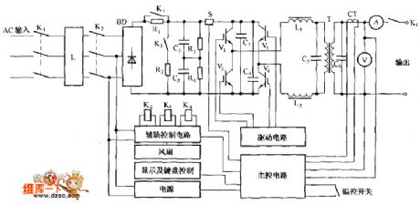
Published:2011/6/20 22:05:00 Author:Seven | Keyword: application circuit
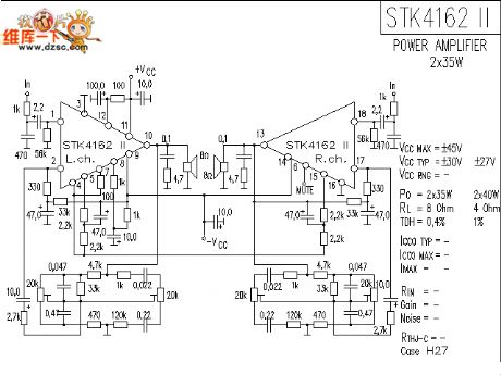
The STK4162 application circuit is shown in theabove figure.
(View)
View full Circuit Diagram | Comments | Reading(3910)
Published:2011/6/21 2:03:00 Author:Seven | Keyword: delayed pulse, generating

In the figure is the delayed pulse generating circuit, this circuit can recognize the reaction time of the ultrasonic. The spread speed of the sound wave is about 340m/s, if the round-trip of the sound wave is 2~20m, then we need 5.88~58.8ms time delay. If the window detection is done, the window width is 10cm~1m, the trigger pulse width Tw is 300μs~3ms. In the circuit, the delay unit is the CMOS single steady multi-resonance oscillator 4538B. The trigger signal makes the transistor VT1 conducting before it triggers the pulse, when the delay unit begins to time, the pulse width Td=C2(R4+RP1).
(View)
View full Circuit Diagram | Comments | Reading(1040)
Published:2011/6/23 19:46:00 Author:Seven | Keyword: parallel connection, controllable silicon circuit
View full Circuit Diagram | Comments | Reading(657)
Published:2011/6/20 22:05:00 Author:Seven | Keyword: ultrasonic wave, remote control
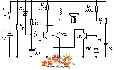
The practical ultrasonic wave remote control emitting circuit is shown in the figure.
(View)
View full Circuit Diagram | Comments | Reading(1234)
Published:2011/6/20 0:57:00 Author:Seven | Keyword: application circuit

The STK4132 application circuit is shown in the figure.
(View)
View full Circuit Diagram | Comments | Reading(5134)
Published:2011/6/23 1:20:00 Author:qqtang | Keyword: self-motivation, power supply

When the power supply is installed, R1 provides with starting current for the switch pipe VT1, and VT1 is conducting, whose collecting electrode current IC is linearly rising in L1, in L2, there inducts a passive forward feedback voltage that the basic pole of VT1 is positive, and the emitter is passive, which makes VT1 saturate quickly. At the same time, the inducting voltage charges C1, as the charging voltage of C1 is rising, the basic pole LEV of VT1 is getting lower, which leads to the saturation of VT1 and VT1 quits the area, IC begins to get lower, and a voltage that the basic pole is passive and the emitter is positive is inducted in L2, so VT1 is blocked quickly. (View)
View full Circuit Diagram | Comments | Reading(676)
Published:2011/6/20 1:33:00 Author:Seven | Keyword: FM modulation, crystal oscillator

In the figure is the FM modulation circuit of crystal oscillator. FM modulation has direct and indirect FM ways, the direct FM method is to directly change the frequency of the oscillating circuit, it's simple, but as it is the LC oscillating circuit, the bias is kind of noticeable, and the stability is weak, i.e the frequency is easy to be affected by the power supply voltage change and the temperature change.
By using the crystal oscillating circuit, the frequency stability is high and the bias is only about 1%. In the circuit, X is a 10MHz crystal oscillator and it directly modulates the frequency of the circuit. (View)
View full Circuit Diagram | Comments | Reading(7179)
| Pages:1729/2234 At 2017211722172317241725172617271728172917301731173217331734173517361737173817391740Under 20 |
Response in 12 hours
© 2008-2012 SeekIC.com Corp.All Rights Reserved.