
Circuit Diagram
Index 1728
The high-voltage generator (555)
Published:2011/6/22 1:10:00 Author:Borg | Keyword: high-voltage generator
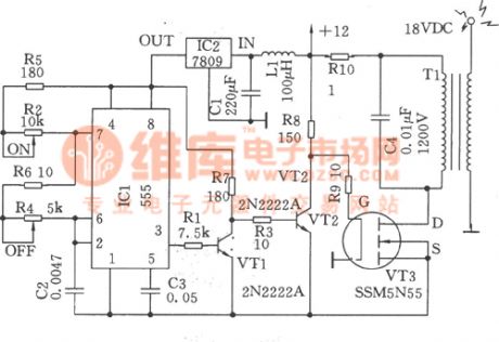
In the figure is the high-voltage generator circuit. This kind of circuit is used in conditions that need high-voltage and low-current, and it can generates high voltages of several thousand and dozens of thousands of volts. The circuit consists of the pulse generator, drive and high voltage transformer. The pulse generator is connected serially with VT1 by a 555 timer. As the buffer, VT1 separates high load resistance of IC1 and IC2 grid. The resistors of R1, R3, R2 and R4 adjust the output pulse frequency of ICI 3-pin.The pulse controls the ON/OFF action of VT3 (View)
View full Circuit Diagram | Comments | Reading(2704)
The AC regulated circuit
Published:2011/6/19 8:51:00 Author:Seven | Keyword: regulated circuit

View full Circuit Diagram | Comments | Reading(591)
The variode FM modulation circut
Published:2011/6/19 10:17:00 Author:Seven | Keyword: FM modulation circut

In the circuit, VT1 magnifies the signal generated by the electret capacitance microphone to the value of the VDc working voltage. The LC oscillating circuit, which is composed of VT2 and so on, generates a 80MHz signal. L1 is the oscillating coil with magnetic cores, which can set the value of the oscillating frequency at 76~90MHz. The frequency of the resonance circuit is changed by the variode VDc, and the frequency is FM modulated directly, when the microphone outputs a 3mV current, we can get a ±25kHz MOD. The FM modulation signal is magnified to about 2.3mV by VT3 and then emitted to the sky by the aerial.
(View)
View full Circuit Diagram | Comments | Reading(786)
The single channel amplifier circuit
Published:2011/6/22 1:11:00 Author:Borg | Keyword: single channel, amplifier

The single channel amplifier circuit (View)
View full Circuit Diagram | Comments | Reading(624)
The DC high voltage generator
Published:2011/6/22 1:16:00 Author:Borg | Keyword: DC, high voltage

In the figure is the DC high voltage generator. It is a small-sized high voltage DC generator, which can generate the DC voltage of 10000V. (View)
View full Circuit Diagram | Comments | Reading(3692)
The DC passive high voltage generator
Published:2011/6/22 1:28:00 Author:Borg | Keyword: DC passive, high voltage
The figured DC passive high voltage generator is specially designed for the high voltage static electricity spraying equipment. The circuit is small-sized and low-power, and its output passive high voltage is stable and adjustable, its maximum output DC is 100,000v. It has functions of overloading protection self-stopping and self-recovering. Elements selecting: T1 is a 30~40W and 2×24V power supply transformer. T2 and T3 are the push transformer of the black-white TV. T4 is the separated line output transformer of 17 inch black-white TV. TV5 can be chosen as 3DDl5D, 3JL06 and so on. RP1 is the multi-turn potentiometer of 20K12. (View)
View full Circuit Diagram | Comments | Reading(794)
The OCL stereo sound power amplifier circuit
Published:2011/6/21 21:34:00 Author:qqtang | Keyword: stereo sound, power amplifier

The OCL stereo sound power amplifier circuit is shown as above.
(View)
View full Circuit Diagram | Comments | Reading(1778)
The block frequency reducing circuit of capacitors (wide band reaction signal regulator 1B31)
Published:2011/6/23 1:06:00 Author:qqtang | Keyword: block frequency, wide band

By the external capacitors CSEL1 and CSEL2, the block frequency of the low-pass filter can be set under 1KHz, which can meet the narrow band need, see as the figure. The capacitance computing formula is as follows.
(View)
View full Circuit Diagram | Comments | Reading(607)
The timer circuit used by TV sets
Published:2011/6/23 6:51:00 Author:qqtang | Keyword: timer circuit

In the circuit is the timer circuit used by TV sets. In the circuit, the current transformer T2 is used to test the current in the power wires while the TV is working, the output of T2 is added on the input terminal of op-amp A1. To prevent A1 from being broken by over input, VD1, VD2, R1 and R2 are used to share the voltage and fulfill the function of protection. R3 provides with a bias voltage which is higher than 7mV for A1, when there is a AC in T2, A1 is outputting a low LEV, the the current is a changing DC, as the time constants of A4 and C1 is large, so A2 is outputting a low LEV while there is a AC in T2.
(View)
View full Circuit Diagram | Comments | Reading(603)
Notch filter with variable Q circuit
Published:2011/6/21 0:53:00 Author:John | Keyword: Notch filter
Notch filter with variable Q circuit is shown.
(View)
View full Circuit Diagram | Comments | Reading(976)
LM387 voice filter circuit
Published:2011/6/15 5:08:00 Author:John | Keyword: voice filter
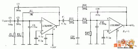
Serial voice filter with a range of voice frequency circuit is shown in the following figure. And its frequency ranges from 360Hz to 3KHz.
(View)
View full Circuit Diagram | Comments | Reading(1804)
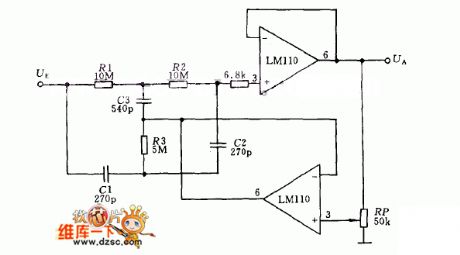
Fourth-order low-pass filter circuit
Published:2011/6/15 10:24:00 Author:John | Keyword: Fourth-order low-pass filter
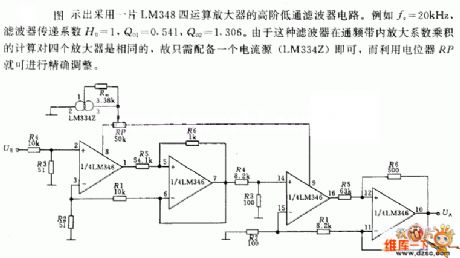
The figure shows a circuit which uses a high-level low-pass filter composed of a piece of LM348 four-operational amplifier. For example, if fc = 20kHz, filter transferring coefficient is counted as H0 = 1, Q01 = 0.541, Q02 = 1.306. Only one current source (LM334Z) is needed to be equipped with the filter because this filter can lead to the same product calculation for four amplifiers within band-pass amplification factor. Potentiometers RP can be used for precision adjustment.
(View)
View full Circuit Diagram | Comments | Reading(1276)
The block frequency rising (wide band reaction signal regulator 1B31) circuit with resistors
Published:2011/6/23 11:24:00 Author:qqtang | Keyword: block frequency, signal regulator, resistor


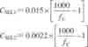
By 3 external resistors, the block frequency can be risen from 1KHz to 20KHz, which can meet the need of wide band. The circuit is shown in the figure. The resistance value computing formulais as follows:
In the formula, the unit of RSEL1~RSEL3 is kΩ. Besides, the resistance valuecan be chosen according to the table.
(View)
View full Circuit Diagram | Comments | Reading(696)
The vehicle battery inverter circuit
Published:2011/6/19 8:55:00 Author:Seven | Keyword: vehicle battery, inverter
The vehicle battery inverter circuit is shown in the figure.
(View)
View full Circuit Diagram | Comments | Reading(875)
the simple LED driver circuit
Published:2011/6/19 8:56:00 Author:Seven | Keyword: LED driver
View full Circuit Diagram | Comments | Reading(849)
The STK4181 application circuit
Published:2011/6/19 9:43:00 Author:Seven | Keyword: application circuit

The STK4181 application circuit is shown in the figure.
(View)
View full Circuit Diagram | Comments | Reading(2473)
The MCl45027 typical application circuit (2)
Published:2011/6/19 9:57:00 Author:Seven | Keyword: typical application circuit
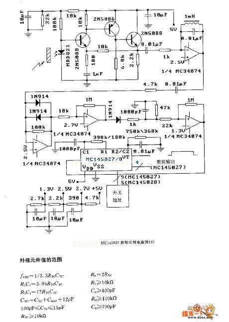
The MCl45027 typical application circuit (2)
The range of external element values (View)
View full Circuit Diagram | Comments | Reading(443)
The MCl45027 typical application circuit (1)
Published:2011/6/19 8:53:00 Author:Seven | Keyword: typical application circuit

The MCl45027 typical application circuit (1) (View)
View full Circuit Diagram | Comments | Reading(481)
The time accumulation circuit
Published:2011/6/22 6:40:00 Author:qqtang | Keyword: time accumulation
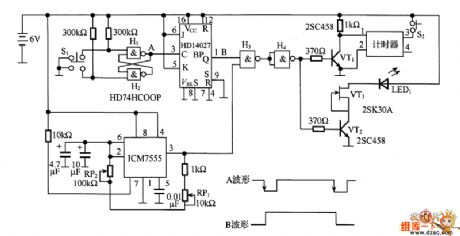
In the figure is the time accumulation circuit. In the circuit, H1 and H2 are vibrations generated by the switch, when the switch of S1 is pressed, it generates a passive pulse and triggers HD14027, and its 1-pin (Q terminal) outputs a high LEV, and the LEV is added on the input terminal of the timer by H3, H4 and VT1, then the timing is starting. ICM7555 composes the multi-resonance oscillator, by changing the RP2, the oscillating frequency is adjusted, the output pulse of the 3-pin of ICM7555 is also added on the input terminal of H3, then the timer begins to time the pulses. When the timing is over, press S1, which generates the passive pulse and triggers HD14027.
(View)
View full Circuit Diagram | Comments | Reading(512)
The MCl45027 pulse waveform and test circuit
Published:2011/6/19 10:00:00 Author:Seven | Keyword: waveform, test circuit
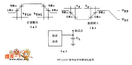
Figure: The MCl45027 pulse waveform and test circuit (View)
View full Circuit Diagram | Comments | Reading(400)
| Pages:1728/2234 At 2017211722172317241725172617271728172917301731173217331734173517361737173817391740Under 20 |
Circuit Categories
power supply circuit
Amplifier Circuit
Basic Circuit
LED and Light Circuit
Sensor Circuit
Signal Processing
Electrical Equipment Circuit
Control Circuit
Remote Control Circuit
A/D-D/A Converter Circuit
Audio Circuit
Measuring and Test Circuit
Communication Circuit
Computer-Related Circuit
555 Circuit
Automotive Circuit
Repairing Circuit