
Circuit Diagram
Index 1727
The step-down switching power supply made of MC34063
Published:2011/6/14 4:19:00 Author:Borg | Keyword: step-down, switching power supply

View full Circuit Diagram | Comments | Reading(4547)
The boosttrapping voltage sawtooth wave generator of 555
Published:2011/6/13 21:00:00 Author:Borg | Keyword: boosttrapping voltage, sawtooth wave
View full Circuit Diagram | Comments | Reading(712)
The adjustable high-voltage regulated power supply circuit (1)
Published:2011/6/19 3:40:00 Author:Seven | Keyword: high-voltage, regulated power supply

The adjustable high-voltage regulated power supply circuit (1) is shown in the figure.
(View)
View full Circuit Diagram | Comments | Reading(875)
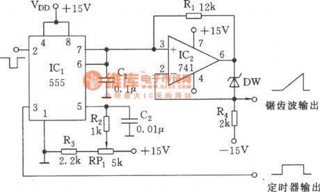
The bootstrapping sawtooth wave generator circuit of 555
Published:2011/6/13 20:59:00 Author:Borg | Keyword: bootstrapping, sawtooth wave generator
View full Circuit Diagram | Comments | Reading(1071)
The output voltage adjustable power supply composed of MAX761
Published:2011/6/14 20:47:00 Author:Borg | Keyword: output voltage, power supply

View full Circuit Diagram | Comments | Reading(560)
The simple frequency splitter circuit composed of SN7474N
Published:2011/6/17 22:19:00 Author:Borg | Keyword: frequency splitter
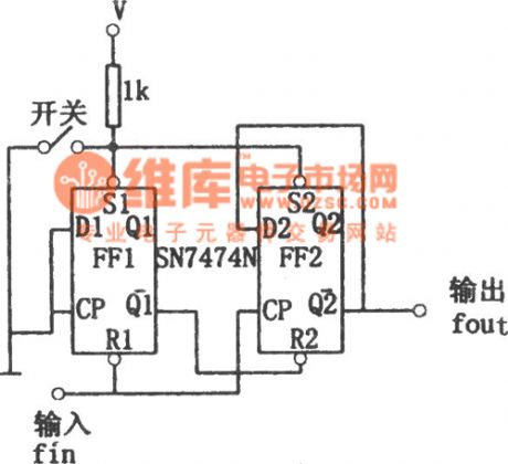
View full Circuit Diagram | Comments | Reading(1109)
The adjustable constant frequency splitter composed of S8424
Published:2011/6/17 21:59:00 Author:Borg | Keyword: adjustable constant, frequency splitter
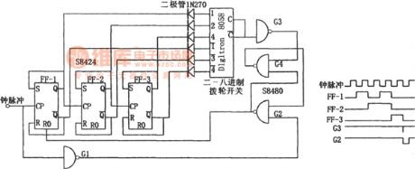
In the figure is the adjustable constant frequency splitter composed of S8424. This circuit consists of R-S trigger, gate circuit and binary-octal dial switch, which can do 1~8 frequency splitting. In the figure, 8058 is the switch, S8424 is the two-team RST trigger. S8480 is the 4*2 inputting NAND. The binary-octal dial switch is used to confirm the constant of the splitter, which makes sure the trigger is reset. If the binary-decimal dial switch is used, then an external trigger and two diodes are needed. (View)
View full Circuit Diagram | Comments | Reading(574)
The simple pulse frequency doubler
Published:2011/6/17 9:11:00 Author:Borg | Keyword: pulse frequency doubler
In the figure is the simple pulse frequency doubler. This circuit is a simple pulse frequency doubler whose output pulse width depends on the time constant RC. By the figured element value, the output pulse width is 1/4 of the input pulse period. To different types of integrated circuit, the values of R and C are different. If the two same circuits are connected in the serial way, a 4-time frequency doubler circuit is formed, but the the second stage time constant RC is 1/2 of the former one. (View)
View full Circuit Diagram | Comments | Reading(2389)
The isolation detection circuit
Published:2011/6/19 8:04:00 Author:Seven | Keyword: isolation detection

The simulation signal detection circuit is to convert the strong signal into the weak digital signals that dsp can read, and it must be sure of the isolation of the strong and weak electricity. The writer chooses the HP hcp17800a photoelectric coupler, whose linearity is 0.004%, and the impedance is 15kv/lμs when the common voltage is 1000v, the gain drift is 0.000 25v/℃, the band width is 100KHz. The concrete isolation detection circuit is shown in the figure.
(View)
View full Circuit Diagram | Comments | Reading(958)
The frequency doubler composed of CMOS elements
Published:2011/6/17 20:03:00 Author:Borg | Keyword: frequency doubler, CMOS
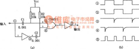
(View)
View full Circuit Diagram | Comments | Reading(1743)
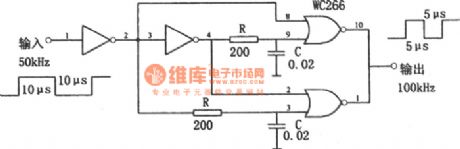
The square wave doubler (SN15844N and SN7400N)
Published:2011/6/17 19:51:00 Author:Borg | Keyword: square wave doubler
In the figure is the square wave doubler. In the circuit, gate G1 is the phaser inverter, the input signal crosses G1 and then in imposed on the input terminal of G2. When the voltage on the two terminals of C1 reaches the G2 threshold voltage, the output of G2 becomes logic 0 , at the moment, C2 discharges with the help of G2. When the input signal comes back to logic 1 , C1 is discharging with the help of G1 and C2 is charged by R2. When the voltage on the two terminals of C2 reaches the threshold voltage, the output of G3 becomes logic 0 . The NAND of G5, G6, 67 and G8 composes the OR gate. (View)
View full Circuit Diagram | Comments | Reading(918)
TGBT drive circuit
Published:2011/6/19 8:17:00 Author:Seven | Keyword: drive circuit

The pwm signal generated by dsp control circuit first crosses the drive circuit, and then controls the ON/OFF state of the igbt switch pipe. The writer chooses HP hcpl3120 specialized igbt drive circuit, see as the figure. The output and input of the drive circuit are isolated to each other, the drive circuit also has the function of LEV switching, it can convert the dsp +5 control voltage in the +15V igbt drive circuit, the drive circuit is equipped with the MORNSUN b0515 isolating power supply module.
(View)
View full Circuit Diagram | Comments | Reading(1798)
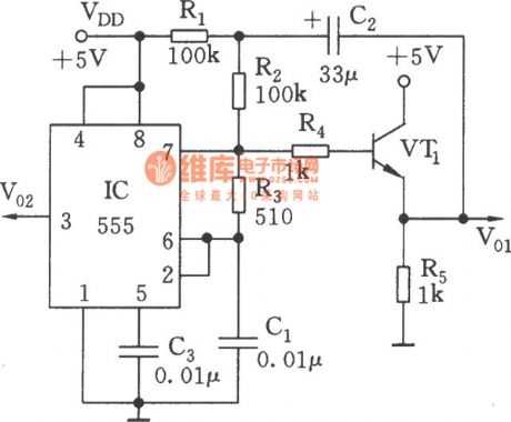
The NE555 FM modulation circuit
Published:2011/6/19 8:33:00 Author:Seven | Keyword: modulation circuit

In the figure is the NE555 FM modulation circuit. In the figure, NE555 7-pin is connected with a FM modulation circuit which is composed with R5 and C2, but the frequency range is kind of small. VT1 and VT2 form a current Miller circuit, which generates a charging current in the charging circuit, the current magnitude is decided by R2 and RP1. The low-frequency modulation signal and the bias current IB are added up and then the oscillating frequency is changed. VT1 and VT2 in the current Miller circuit would better be couple pipe.
(View)
View full Circuit Diagram | Comments | Reading(5633)
The low-noise ECC83 headphone amplifier circuit and el84 valve
Published:2011/6/22 1:48:00 Author:Borg | Keyword: low-noise, headphone amplifier
View full Circuit Diagram | Comments | Reading(3253)
The AT-HA2002 amp audio part principle circuit
Published:2011/6/21 10:04:00 Author:Borg | Keyword: amp, audio part, principle circuit
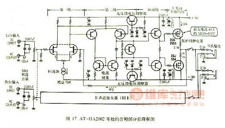
Figure 17. The AT-HA2002 amp audio part principle circuit (View)
View full Circuit Diagram | Comments | Reading(1704)
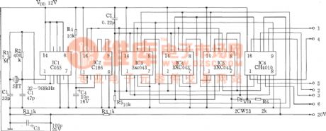
The 3-phase signal generator
Published:2011/6/21 9:49:00 Author:Borg | Keyword: 3-phase, signal generator
View full Circuit Diagram | Comments | Reading(1439)
The PCL86 cow output amp circuit
Published:2011/6/21 9:57:00 Author:Borg | Keyword: output amp

View full Circuit Diagram | Comments | Reading(4589)
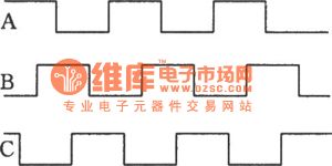
The 3-phase square wave generator
Published:2011/6/21 10:00:00 Author:Borg | Keyword: 3-phase, square wave
View full Circuit Diagram | Comments | Reading(1398)
The FM modulation circuit composed of transistors
Published:2011/6/19 8:48:00 Author:Seven | Keyword: FM modulation circuit, transistors

In the circuit, VT2 and VT3 are the multi-resonance oscillator circuit which is coupled by emitters, VT4 and VT5 compose the constant current circuit, which is controlled by the current. By using the clamp diodes of VD2 and VD3 which rise the switch shifting speed, the collecting electrode voltage fluctuation of VT2 and VT3 is kept at 0.5~0.6V. By the figured parameter, when the bias voltage is 5V, the oscillating frequency is f0=3.3×10/C2, and the temperature coefficient is positive to the outside temperature. Because the temperature coefficient of the basic pole-emitting pole voltage UBE of the transistor is passive, then emitting pole current has the positive coefficient.
(View)
View full Circuit Diagram | Comments | Reading(1109)
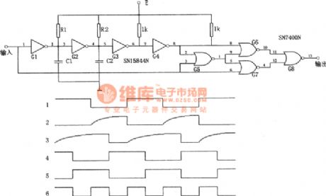
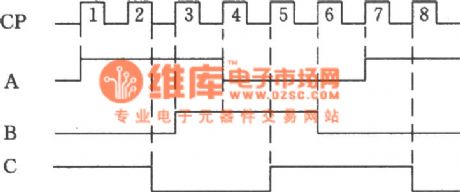
The 3-phase square wave signal oscillator
Published:2011/6/22 0:58:00 Author:Borg | Keyword: 3-phase, square wave, signal oscillator
In the circuit is a gundam senary counter which is composed of a CD4017, the input clock frequency is 300Hz, VDl~VD9 and R1~R3 compose 3 s-phase input OR gates, they pick out the 3-phase square wave signals whose difference is 120o and the frequency is 50Hz. The 3-phase signal can be got from either A, B or C. The waveform are shown here.
(View)
View full Circuit Diagram | Comments | Reading(1454)
| Pages:1727/2234 At 2017211722172317241725172617271728172917301731173217331734173517361737173817391740Under 20 |
Circuit Categories
power supply circuit
Amplifier Circuit
Basic Circuit
LED and Light Circuit
Sensor Circuit
Signal Processing
Electrical Equipment Circuit
Control Circuit
Remote Control Circuit
A/D-D/A Converter Circuit
Audio Circuit
Measuring and Test Circuit
Communication Circuit
Computer-Related Circuit
555 Circuit
Automotive Circuit
Repairing Circuit