
Index 49
Unity_gain_inverting_wideband_amplifier
Published:2009/7/23 20:57:00 Author:Jessie
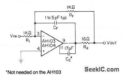
This circuit shows the basic connections in a typical unity-gain inverting amplifier. The use of a compensation capacitor Cc is required for the AN104, unless the gain is fairly high. The AN103 only needs additional external compensation in special cases, such as when used as a noninverting unity-gain follower. Rd in the output circuit improves frequency stability. CF compensates for a pole in the closed-loop transfer function, caused by the input capacitance and feedback resistors. A ground plane is recommended, leads must be short, and Rf should not exceed 5.6 kΩ. Typical bandwidth is 35 MHz, with slew rates of 230 V/μs, into a 330-Ω load (View)
View full Circuit Diagram | Comments | Reading(705)
Ac_coupled_video_amplifier_with_single_supply
Published:2009/7/23 20:56:00 Author:Jessie

This circuit can be used in ac applications, such as video amplifiers and active filters, but requires only one supply. The output swing is over 8 Vpp with a 12-V supply. Input impedance is about 500 kΩ. (View)
View full Circuit Diagram | Comments | Reading(576)
Ac_coupled_video_amplifier_with_high_input_impedance
Published:2009/7/23 20:55:00 Author:Jessie

This circuit can be used in ac applications, such as in video amplifiers and active filters. The circuit uses boot-strapping to achieve input impedances in excess of 10 MΩ. (View)
View full Circuit Diagram | Comments | Reading(523)
Shield_or_line_driver_for_high_speed_video_applications
Published:2009/7/23 20:54:00 Author:Jessie
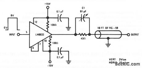
This circuit uses the low input current, high speed, and high-capacitance drive capabilities of the LH0033 to full advantage for high-speed video applications, such as in automatic test equipment. In this circuit, the LH003 is. mounted close to the device under test, and drives the cable/shield, thus allowing higher-speed operation because the device under test does not have to charge the cable. (View)
View full Circuit Diagram | Comments | Reading(539)
JFET_bipolar_cascode_video_amplifier
Published:2009/7/23 20:51:00 Author:Jessie

This cascode circuit provides full video output for the CRT cathode drive. Gain is about 90. The cascode configuration eliminates Miller-capacitance problems with the JFET, thus allowing direct drive from the video detector. An m-derived filter, which uses stray capacitance and a variable inductor, prevents a 4.5-MHz sound frequency from being amplified by the video amplifier. (View)
View full Circuit Diagram | Comments | Reading(0)
MAGNETIC_TAPE_FLAW_DETECTOR
Published:2009/7/23 21:52:00 Author:Jessie
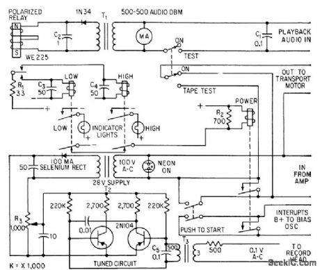
Transistor oscillator records steady test lone on tape. Machine stops during playback when repro-duced level indicates law that would make tape unsuitable for broadcast use. Polarized relay charges memory capacitor as it responds to transient. Capacitor discharges into coil of slower relay, which in turn slops transport. -N. J. Thompson, Detector Pin-Points Magnetic Tape Flaws, Electronics, 32:2, p 50-51. (View)
View full Circuit Diagram | Comments | Reading(889)
TRANSISTORIZED_UHF_TV_TUNER
Published:2009/7/23 21:52:00 Author:Jessie
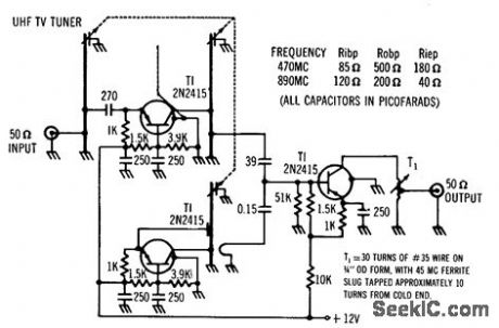
Gain is 3 to 9 db over tuning range of 470 to 890 Mc and noise-figure is 7 to 9 db, with output at 45 Mc. Current drain is only 18 ma at 12 v.-Transistorized UHF Tuner Features Low Noise, High Gain, Electronics, 36:2, p 15. (View)
View full Circuit Diagram | Comments | Reading(2515)
Miniature_AM_radio_receivers
Published:2009/7/23 21:48:00 Author:Jessie
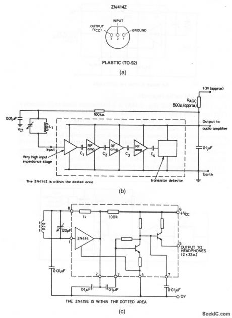
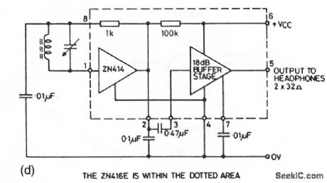
The ZN414Z (Fig. 2-14A) is a 10-transistor tuned-radio-frequency (TRF) circuit in a 3-pin TO-92 plastic package (Fig. 2-14B). The ZN414Z provides a complete RF amplifier, detector and AGC circuit that requires only six external components to produce an AM tuner. AGC action is adjusted by selecting one external resistor value. Current consumption is low (typically 2 to 4 mA), and no set-up or alignment is required. The ZN415E (Fig. 2-14C) retains all the features of the ZN414Z, but also includes a buffer stage that is capable of driving headphones directly. The ZN416E (Fig. 2-14D) is also a buffered-output version of the ZN414Z, which provides a typical 120 mV (rms)output into a 64-Ω load. (View)
View full Circuit Diagram | Comments | Reading(1397)
MEASURING_SCR_TURNOFF_TIME
Published:2009/7/23 21:48:00 Author:Jessie

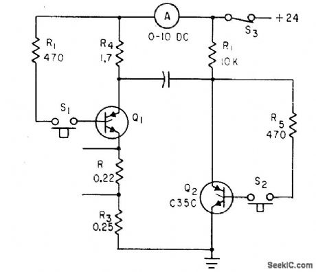
Q1 in parallel inverter circuit is triggered by dosing S1, to give 10 amp of test current. When S2 is closed after warmup, Q2 turns on, connects positively charged plate of C1 to cathode of Q1, and makes reverse current flow. If turnoff lime of Q1 is less than 12 microsec, it will remain turned off and ammeter reading will return to zero. If test rectifier fails to turn off, S3 should be opened immediately each drive monostable mvbr, with output to prevent overheating.-D. V. Jones, Turn-Off Circuits for Controlled Rectifiers, Electronics, 33:32, p 52-55.
(View)
View full Circuit Diagram | Comments | Reading(632)
IMPROVED_CODAN
Published:2009/7/23 21:48:00 Author:Jessie
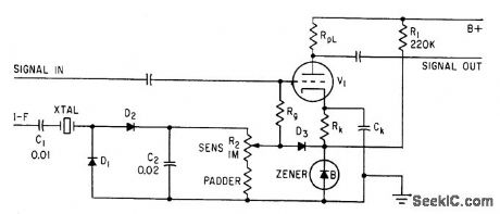
Applied to first audio tube of receiver. Tube is biased off by zener diode in cathode circuit, and keep alive current is supplied to zener from B+. Actuating codan, consisting of crystal, voltage-doubling rectifier, smoothing capacitor C2, and load, produces positive output only when signal is received from i-f. Crystal is at 1.1 center frequency. Audio is thus unblocked only when voltage of desired signal, as set by R2, is sufficient to overcome cutoff bias in cathode circuit.-R. L. Ives, Crystal Codans Give Accurate Receiver Tuning, Electronics, 33;22, p 113. (View)
View full Circuit Diagram | Comments | Reading(684)
Switching_time_tests
Published:2009/7/23 21:48:00 Author:Jessie

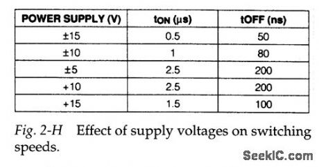
Figure 2-G shows a test circuit and waveforms for measuring switching time for the MAX326/27 .As a point of reference, tON should be between 500 and 1000 ns, with tOFF between 50 and 500 ns. Figure 2-H shows how switching speeds are affecter by supply voltages.
(View)
View full Circuit Diagram | Comments | Reading(547)
Off_channel_leakage_tests
Published:2009/7/23 21:44:00 Author:Jessie

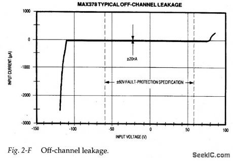
Figure 2-E is a test circuit for measuring off-channel input voltage versus the resulting input-leakage current. Figure 2-F shows typical test results. As shown, the input leakage during fault conditions is less than 20nA. The voltmeter at the out-put shows the effect of off-channel leakage on the selected channel. The effect with 100-kΩ, input resistors (less than 0.1 mV) is hardly noticeable.VOUT is limited by internal clamps to about 3 V less than the supply rails, and ranges between ±12 V with ±15-V supplies. VOUT collapses to 0 V when the power is off.
(View)
View full Circuit Diagram | Comments | Reading(763)
High_speed_video_peak_detector
Published:2009/7/23 21:15:00 Author:Jessie
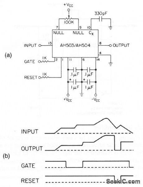
This circuit shows an AH503 or AH504 connected as a video-peak sensor or detector, using a minimum of extemal components. Figure 3-60B shows the related waveforms. The circuit will accommodate a 10-V pulse, and will capture individual 1-V pulses as narrow as 100 ns to within ± 10 mV. Delay between input peak and output settling is 500 ns. (View)
View full Circuit Diagram | Comments | Reading(552)
20_MHz_video_log_amplifier
Published:2009/7/23 21:12:00 Author:Jessie

This circuit shows a 2920 in the basic log-amplifier configurations, using a minimum of external components. The offset pot between pins 9 and 10 is mandatory. Vcc is typically±15 V, C2 is typically between 10 and 50 pF. The circuit has a 20-MHz bandwidth and an 80-dB dynamic range. (View)
View full Circuit Diagram | Comments | Reading(606)
PORTABLE_TV_TUNER
Published:2009/7/23 21:39:00 Author:Jessie
Three transistors in vhf tuner provide 19 db power gain even for channel 13, with 12 db noise factor. V. Mukai and P. V. Simpson, Transistorized Tuners For Portable Television, Electronics, 33:12, p 76-78. (View)
View full Circuit Diagram | Comments | Reading(2226)
Balanced_high_level_mixer
Published:2009/7/23 21:42:00 Author:Jessie
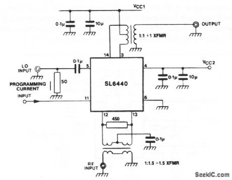
This circuit shows the SL6440 (Fig. 2-10) with a balanced input (for improved carrier leak), and balanced output (for increased conversion gain). A lower VCC can be used with this arrangement (for lower device dissipation).Conversion gain for the balanced circuit of Fig. 2-11 is equal to: Gdb 20=20 Log56.61 IP+0.0785,2RLIP.where IP is programmed current at pin 11, and RL is dc load resistance. (View)
View full Circuit Diagram | Comments | Reading(1047)
AUTOMATIC_BRIGHTNESS_CONTROL
Published:2009/7/23 22:59:00 Author:Jessie
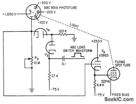
Automatic brightness control circuit intensifies scanning spot when sweep is triggered, and holds intensity constant. When spot is quiescent, output of 931A is applied to cathode follower that determines bias on 5ZP16.Phototube then sees only 10-meg load because V4 is cut off. When mark is sensed by scanner, load switching action makes V4 conduct to reduce phototube load to 120,000 ohms.-A. C. L. Brown, Flying Spot Inspects TV Rating Records, Electronics, 35:9, p 31- 34. (View)
View full Circuit Diagram | Comments | Reading(1162)
FERRITE_CUP_TUNER
Published:2009/7/23 21:46:00 Author:Jessie
Rotary-axial tuner consists of two pairs of ferrite cups with ground D-shaped center cores, ganged to produce linear frequency variation from 500 to 1,600 kc with 270℃ rotation, Operating frequencies can be extended to 15 Mc.-E. A. Abbot and M. Lafer, Miniature Ferrite Tuner Covers Broadcast Band, Electronics, 31;9, p 72-73. (View)
View full Circuit Diagram | Comments | Reading(633)
electronic sterilizer circuit diagram
Published:2011/7/13 9:36:00 Author:Nancy | Keyword: electrpnic sterilizer
View full Circuit Diagram | Comments | Reading(2095)
AM_IF_and_detector_with_noise_blanker
Published:2009/7/23 21:45:00 Author:Jessie
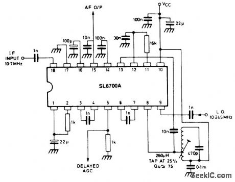
The SL6700 shown is similar to the SL6701 (Fig. 2-12), but with the addition of a noise blanker. The circuit shown in Fig. 2-13 is for an AM double-conv ersion receiver with noise blanker. (View)
View full Circuit Diagram | Comments | Reading(2165)
| Pages:49/126 At 204142434445464748495051525354555657585960Under 20 |
Circuit Categories
power supply circuit
Amplifier Circuit
Basic Circuit
LED and Light Circuit
Sensor Circuit
Signal Processing
Electrical Equipment Circuit
Control Circuit
Remote Control Circuit
A/D-D/A Converter Circuit
Audio Circuit
Measuring and Test Circuit
Communication Circuit
Computer-Related Circuit
555 Circuit
Automotive Circuit
Repairing Circuit