
Index 48
Low_distortion_bridge_audio_power_amplifier
Published:2009/7/23 21:09:00 Author:Jessie

This circuit is capable of 40-W into an 8-Ω speaker, or 28-W into a 16-Ω speaker, with a voltage gain of 3 and a full-power bandwidth from dc to 100 kHz. Figures 1-44B and 1-44C show the circuit performance characteristics. (View)
View full Circuit Diagram | Comments | Reading(674)
Wideband_amplifier_for_test_equipment_applications
Published:2009/7/23 21:09:00 Author:Jessie
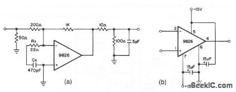
This circuit shows a 9826 used in an application where high speed at a relatively low gain is required (a gain of 5 in this case). Rx and Cx form a lead/lag network between the inverting and noninverting inputs. With the values given, this circuit can operate comfortably at frequencies of 20 MHz. If a lower gain is needed (gain less than 5), connect a 1- to 5-pF capacitor between the output and inverting input to aid in suppressing parasitic oscillations. The 100-Ω 5-pF filter at the output has a damping effect to help suppress signal overshoot. Figure 3-54B shows external connections for the 9826. (View)
View full Circuit Diagram | Comments | Reading(604)
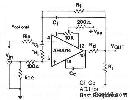
Wideband_difference_amplifier
Published:2009/7/23 21:08:00 Author:Jessie
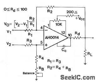
This circuit shows an AH0014 connected as a basic differential or instrumentation amplifier with a balance adjustment. The balance resistor is adjusted for best common-mode rejection ratio. Figure 3-48B shows external connections for the AH0014. (View)
View full Circuit Diagram | Comments | Reading(586)
DIODE_MODIFIED_SCHMITT_TRIGGER
Published:2009/7/23 2:08:00 Author:Jessie
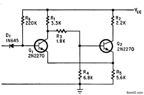
Addition of Rb and D1 reduces loading on driving circuit when Q1 is on, there by preventing input signal from being clamped. Same signal may therefore drive other Schmitt triggers having higher trigger levels.-J. Gaon, Diode and Resistor Increase Input Resistance of Schmitt, Electronics, 39:12, p 110-111. (View)
View full Circuit Diagram | Comments | Reading(725)
High_impedance_low_capacitance_video_buffer
Published:2009/7/23 20:16:00 Author:Jessie
This compound series-feedback circuit provides high input impedance and stable, wideband unity gain for general-purpose video-buffer applications. (View)
View full Circuit Diagram | Comments | Reading(606)
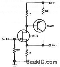
FET_cascode_video_amplifier
Published:2009/7/23 20:14:00 Author:Jessie
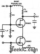
This circuit features very low input loading, and reduction of feedback to almost zero. The 2N3823 is used because of the low capacitance and high Yfs. Amplifier bandwidth is limited by RL and by the load capacitance.
(View)
View full Circuit Diagram | Comments | Reading(0)
Video_coaxial_line_driver
Published:2009/7/23 20:34:00 Author:Jessie
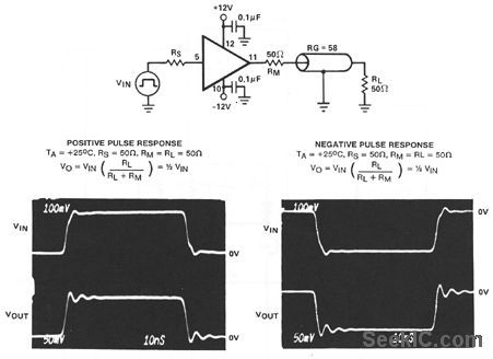
This circuit uses an HA-5033 video buffer as a coax line driver. Notice that both the positive and negative pulse-response waveforms are also shown. The connections given are for the TO-8 metal-can version of the HA-5033.
(View)
View full Circuit Diagram | Comments | Reading(556)
Composite_video_sync_separator
Published:2009/7/23 20:27:00 Author:Jessie

This circuit uses an HA-2544 video op amp (Fig. 3-29) to separate the TV sync signal from the video and blanking signal with a minimum of external components. (View)
View full Circuit Diagram | Comments | Reading(1360)
75_Ω_differential_input_buffer
Published:2009/7/23 20:25:00 Author:Jessie
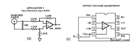
This circuit uses an HA-2544 video op amp to buffer between a 75-Ωline and other video circuits,with a GBW(gain-bandwidth)up to 50MHz.Figure3-29B shows an offset adjustment(if required). A typical range for RT is 20 M. (View)
View full Circuit Diagram | Comments | Reading(544)
12_BIT_BINARY_2s_COMPLEMENT_D_A_CONVERSION_SYSTEM
Published:2009/7/6 3:25:00 Author:May

The front end of the DAC is configured differentially using dual eight-input IC multiplexer 1H6216 and three LM156 op amps. Following the differential amplifier is the programmable gain stage discussed earlier, with a low-pass filter on the output feeding the IH5110 sample and hold amplifier. The output of the IH5110 is connected to the comparator input, - input LM301, through the internal10-KΩ feedback resistor of the 7541 multiplying d/a converter. The AD7541, along with a ±10-V reference and successive approximation logic, make up the 2's complement a/d converter. (View)
View full Circuit Diagram | Comments | Reading(1817)
8_to_1_video_switch_amplifier
Published:2009/7/23 20:43:00 Author:Jessie

This circuit uses two CA3256 ICs to provide an 8-to-1 video-switch function. The analog switches of channels 1 to 8 are digitally controlled by logic, as shown in the truth table. As in the case of the switch circuits shown in Figs. 3-35 through 3-37, the circuit of Fig. 3-38 has programmable gain for all channels, as well as flexible output-voltage swing. Typically, the output voltage swing can be about 5 Vpp, with a Vcc to VEE range of 12 V or greater, and each amplifier can provide a gain of 1 into a 75-Ω load, or a gain of 5 into a 1-kΩ load. (View)
View full Circuit Diagram | Comments | Reading(947)
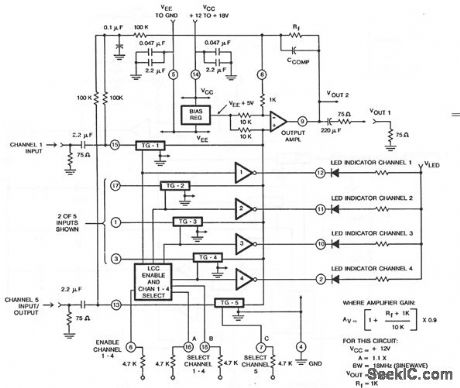
Analog_video_switch_and_amplifier_with_direct_coupled_input_and_output
Published:2009/7/23 20:42:00 Author:Jessie

This circuit shows a CA3256 switch/amplifier connected for a direct-coupled input and output. One of four channels can be selected in parallel with channel 5. The analog switches of channels 1 to 4 are digitally controlled by logic (Fig. 3-35B). A VEE of -5 V is required. The peak-to-peak output voltage is fixed by the Vcc and VEE range, and is about +3.6 to -2.5 V (clipped) for a Vcc of +5 V and a VEE of -5 V. For a 2-Vpp output, Vcc must be +4V, and VEE must be -4 V. This produces a bandwidth of about 10 MHz. Higher Vcc produces greater bandwidths, as shown. (View)
View full Circuit Diagram | Comments | Reading(685)
Analog_video_switch_and_amplifier_with_ac_coupled_input
Published:2009/7/23 20:40:00 Author:Jessie
This circuit shows a CA3256 switch/amplifier connected for an ac coupled input. One of four channels can be selected in parallel with channel 5. The analog switches of channels 1 to 4 are digitally controlled by logic (Fig. 3-35B).Vcc can be from + 12 to + 18 V.VEE is grounded, Amplifier gain is determined by external resistor Rf, as shown by the equation. A typical value of CCOMP is 6 pF. (View)
View full Circuit Diagram | Comments | Reading(653)
Analog_video_switch_and_amplifier_with_direct_coupled_output
Published:2009/7/23 20:38:00 Author:Jessie

This circuit shows a CA3256 switch/amplifier connected for a direct-coupled output. One of four channels can be selected in parallel with channel 5. The analog switches of channels 1 to 4 are digitally controlled by logic (Fig. 3-35B). A VEE of -5 V is required. Vcc can be from +5 to +12 V. Amplifier gain is determined by the external resistor Rf, as shown by the equaeion. (View)
View full Circuit Diagram | Comments | Reading(657)
Single_chip_TV_chroma_luma_processor
Published:2009/7/23 20:36:00 Author:Jessie

The CA3217E contains all required circuit functions between the video detector and picture-tube RGB driver stages of a color television receiver. The CA3217E decodes the chroma signals and then produces three different color signals that are internally combined with the luma to develop the RGB signals. The picture saturation, hue, and brightness controls are externally adjustable by the viewers. The AFPC, ACC, dynamic flesh control, beam limiting, and gate black-level (brightness) controls are servo loops that are used to stabilize the RGB output and reduce frequent manual adjustment. The automatic beam-limiter circuit reduces picture contrast and brightness to prevent excessive drive output at the picture tube. (View)
View full Circuit Diagram | Comments | Reading(1368)
Noninverting_amplifier_for_gains_less_than_10
Published:2009/7/23 21:07:00 Author:Jessie
This circuit shows an AH0014 connected as a noninverting wideband amplifier, where gains must be less than 10, but more than 1. The characteristics are the same as for the circuits of Figs. 3-49 and 3-51. Figure 3-48B shows external connections for the AH0014. (View)
View full Circuit Diagram | Comments | Reading(513)
Noninverting_amplifier_for_gains_greater_than_10
Published:2009/7/23 21:05:00 Author:Jessie
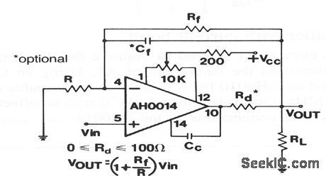
This circuit shows an AH0014 connected as a noninverting wideband amplifier, where gains must be greater than 10. The characteristics are the same as for the circuit of Fig. 3-49. Figure 3-48B shows external connections for the AH0014. (View)
View full Circuit Diagram | Comments | Reading(473)
TV_video_IF_amplifier_and_synchronous_detector_for_cable_receivers
Published:2009/7/23 20:50:00 Author:Jessie

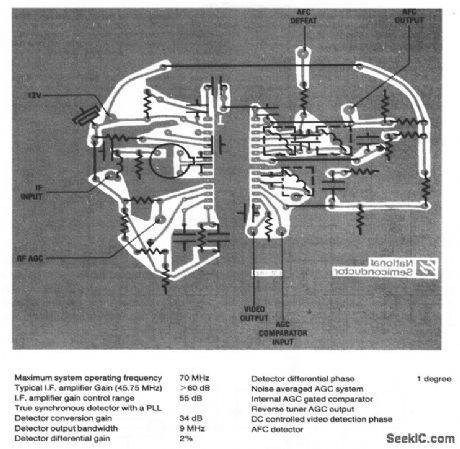
This circuit shows the external connections for an LM1823, which is a video IF amplifier that is designed to operate at intermediate carrier frequencies up to 70 MHz, and use phase-locked loops (PLLs) for synchronous detection of amplitude modulation on these carrier frequencies. Figure 3-39B shows a typical PC layout, and Fig .3-39C tabulates the circuit characteristics. (View)
View full Circuit Diagram | Comments | Reading(700)
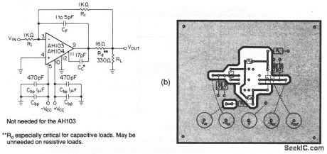
High_gain_video_amplifier
Published:2009/7/23 21:00:00 Author:Jessie

This circuit shows an AH104 used as a high-gain video amplifier. The high output-current capability makes the AH104 suitable for such high-frequency driver applications. In this circuit, a closed-loop gain of 60 can be obtained to 10MHz. For lower gains, Cc must be larger to promote stability. The power connections are the same as for Fig. 3-45. The AN103 can be used in this circuit, without Cc, but the internal 20-pF compensation capacitor reduces the gain at any given bandwidth. (View)
View full Circuit Diagram | Comments | Reading(560)
Video_pulse_amplifier
Published:2009/7/23 20:59:00 Author:Jessie
This circuit shows a video pulse amplifier that uses the basic circuit of Fig. 3-44. Figure 3-45B shows a suggested PC layout. Notice that internal current-limiting resistors provide short-circuit protection to the common line, with a limit of 100-mA maximum. A short to either supply line can destroy the unit.Typical supply voltages are± 20 V. (View)
View full Circuit Diagram | Comments | Reading(571)
| Pages:48/126 At 204142434445464748495051525354555657585960Under 20 |
Circuit Categories
power supply circuit
Amplifier Circuit
Basic Circuit
LED and Light Circuit
Sensor Circuit
Signal Processing
Electrical Equipment Circuit
Control Circuit
Remote Control Circuit
A/D-D/A Converter Circuit
Audio Circuit
Measuring and Test Circuit
Communication Circuit
Computer-Related Circuit
555 Circuit
Automotive Circuit
Repairing Circuit