
Index 47
Wideband_log_amplifier
Published:2009/7/22 6:41:00 Author:Jessie
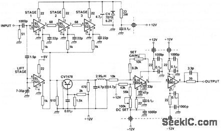


This circuit consists of six log stages (two stages in each dual SL523) and two lift stages, which gives an overall dynamic range of greater than 80 dB. Both the dc level and gain of the video output are adjustable. (View)
View full Circuit Diagram | Comments | Reading(588)
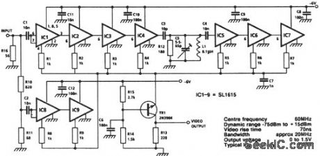
Simple_log_IF_strip
Published:2009/7/22 6:40:00 Author:Jessie


The SL523 shown In this figure is similar to the SL521 shown in Fig.3-2,except that the SL523 is a dual amplifier and provides an approximate 24~dB gain. Typical value for the supply decoupling capacitor is 3 nF. (View)
View full Circuit Diagram | Comments | Reading(667)
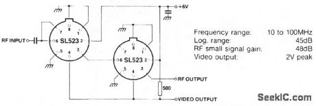
Direct_coupled_wideband_log_amplifier
Published:2009/7/22 6:38:00 Author:Jessie


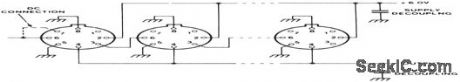
The SL521 shown in this figure is intended primarily for use in successive-detection log IF strips, operating at center frequencies between 10 and 100 MHz. The SL521 is suitable for direct-coupling, and includes a built-in 500-pF supply-decoupling capacitor. Typical stage voltage-gain is 10 to 12 dB. The RF output is taken from pin 4, and the detected output is taken from pin 3. When more than two untuned stages are used, additional decoupling might be required. The values for decoupling capacitors with untuned cascades are: 3 stages 1 nF, 4 stages 3 nF, 5 stages 10 nF, 6 or more stages 30 nF. (View)
View full Circuit Diagram | Comments | Reading(546)
Logarithmic_limiting_amplifier
Published:2009/7/22 6:36:00 Author:Jessie
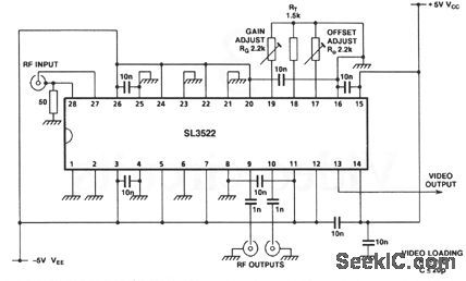
The SL3522 shown in this figure is a 7-stage succes sive-detection log amp for use in the 100- to 600-MHz range. With the values shown, the frequency range is 500 MHz, with a 40-MHz video bandwidth, and a 450-MHz balanced RF bandwidth. Both video gain and offset are adjustable. Gain has an effect on offset, but not vice versa. Typical dynamic range is 75 dB. (View)
View full Circuit Diagram | Comments | Reading(628)
BLOOD_PRESSURE_MONITOR
Published:2009/7/22 6:10:00 Author:Jessie

Continuous indication of blood pressure, with 3% fullscalle accuracy is obtained by mounting variable-reactance pressure transducer in 5-cc syringe inserted directly into patient’s artery Instrument has ranges, for 0-75,0-150,and 0-300mm Hg .Transducer is excited by low-distortion sine wave generated by transistor counterpart of vacuum-tube Wien-bridge oscillator, positive and negative feedback circuits generate 5-kc signal at 1V rms, -O. Z. Roy and J. R. Charbonneau, Transistor Unit Monitors Blood Pressure,Electronic,31:33,p82-83. (View)
View full Circuit Diagram | Comments | Reading(3455)
Strobeflash_slave_adapter
Published:2009/7/22 21:34:00 Author:Jessie
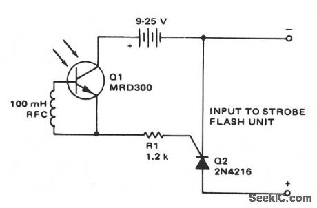
This circuit provides the drive needed to trigger a slave strobeflash, without wires between the master and slave units. When light from the master strobeflash strikes Q1, Q2 is triggered, which applies power to the slave unit. (View)
View full Circuit Diagram | Comments | Reading(560)
OPTOISOLATOR_DRIVES_1_A_POWER_TRANSIS_TOR_IC
Published:2009/7/6 7:32:00 Author:May
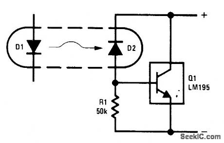
Practically any standard optoisolator provides sufficient output to meet input current requirement of power transistor IC capable of handling 1 A. With no drive, R1 absorbs base current of at, holding it off. When power is applied to LED D1, less than 20μA from photo-diode D2 is sufficient to turn LM195 fully on. Supply can be up to 42 V.- Linear Applications, Vol. 2, National Semiconductor, Santa Clara, CA, 1976, AN-110, p 5. (View)
View full Circuit Diagram | Comments | Reading(650)
DIELECTRIC
Published:2009/7/22 23:08:00 Author:Jessie
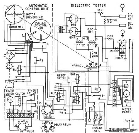
Automatic sequencing of test functions minimizes high-voltage danger to operator and improves accuracy of readings. Control system maybe inserted in any commercial high-pot tester. -F. J. Clounie, P. M. Degroat, and E. M. Szymanski, Control Makes Test Safe, Accurate, Electronics, 33:19, p 88-91. (View)
View full Circuit Diagram | Comments | Reading(772)
AUTOMATIC_BETA_CHECKER
Published:2009/7/22 23:02:00 Author:Jessie
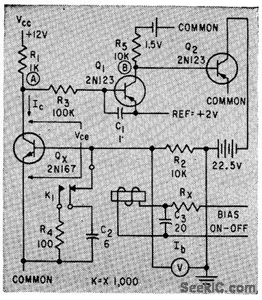
Holds collector current of test transistor Qx at preset value while base current is measured and bola de, termined.-E. P. Hojak, Automatic Measurement of Transistor Beta, Electronics, 32:49, p 114-115. (View)
View full Circuit Diagram | Comments | Reading(675)
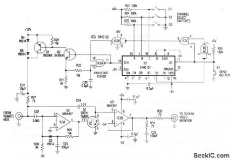
Video_system_channel_control_box
Published:2009/7/22 22:39:00 Author:Jessie

In the channel control box of the single-coax video system (Fig. 3-14), a desired channel is encoded by three bits, set either by switches (as shown) or by an applied digital input. Momentary depression of the send button triggers down-converter IC1 and gated oscillator IC2A to initiate a channel-selection burst.Supply current flows to the remote multiplexor box through Q1 (normally on and saturated), R27, and the coax center conductor. R27 also terminates the coax via C21. When Q1 turns off momentarily, forward bias across D3 and D4 develops a negative 1.2-V channel-select pulse. This 1.2-V drop in supply voltage does not affect the remote multiplexer video output. Consequently, the video monitor display does not flip during channel changes, provided that the channel signals have common sync timing. The short time constant that is associated with coupling of video to the coax (C11 and R9, R27) enables selection of any channel in less than one second, but also allows the video sync-pulse baseline to shift with picture content. To prevent this shift, peak detector IC3A drives Q3, which applies dc restoration ahead of IC3B. During each negative sync pulse, Q3 turns on just long enough to reclamp the pulse tip at 0 V. (View)
View full Circuit Diagram | Comments | Reading(980)
Video_amplifier_dc_stabilizer_differential_inputs
Published:2009/7/22 22:29:00 Author:Jessie
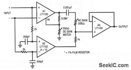
This circuit shows a way to get full differential inputs with dc-stabilized operation. A1 and A2 both (differentially) sense the input at gains of 10. The A3 output is an undistorted, amplified version (in this case, time 10) of the input. The circuit is adjusted by applying a square wave and adjusting the ac gain for the squarest comers, and the dc gain-match for a flat top. Circuit bandwidth exceeds 35 MHz, slew rate is 450 V/μs, and dc offset is about 200μV. (View)
View full Circuit Diagram | Comments | Reading(606)
Video_amplifier_dc_stabilizer_servo_controlled_FET
Published:2009/7/22 22:27:00 Author:Jessie
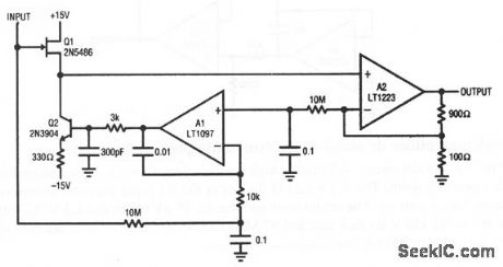
This circuit is a wideband, highly stable, gain-of-10amplifier with high input impedance. Input capacitance is about 3 pF. A2 provides a 100-MHz bandwidth gain of 10 (using the values shown). With an input capacitance of 3 pF and bias current of 100 pA, the circuit is well suited to a variety of video applications. (View)
View full Circuit Diagram | Comments | Reading(742)
Video_amplifier_dc_stabilizer_differentially_sensed_technique
Published:2009/7/22 22:21:00 Author:Jessie
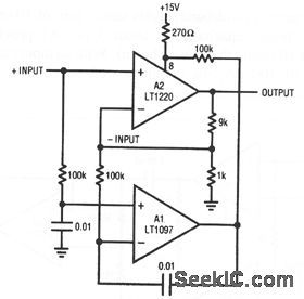
In this circuit, sensing is done differentially, preserving access to both fast amplifier inputs. A1 measures the dc error at the A2 input, and biases the offset pins to force offset within 50 μV. The offset-pin biasing at A2 is arranged so that A1 is always able to find the servo point. The 0.01-μF capacitors rolls off Al at the low frequency, and A2 handles the high-frequency signals. The combined characteristics yield: gain-bandwidth of 45 MHz, offset voltage of 50 μV, offset drift of 1 μV/℃, and a slew rate of 250 V/μs.
(View)
View full Circuit Diagram | Comments | Reading(593)
WAVEFORM_TESTER
Published:2009/7/22 22:20:00 Author:Jessie
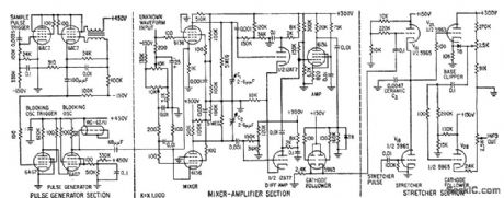
Used in high-speed testing of ferrite cores, transistors, transformers, and other components requiring waveform measurement. Based on sampling of un known waveform at discrete intervals and comparing resulting digital output with that provided by perfect component.-B. Agusta, Sorting Components by Measuring Waveforms, Electronics, 32:7, p 56-59. (View)
View full Circuit Diagram | Comments | Reading(624)
ARMATURE_TESTING_BRIDGE
Published:2009/7/22 22:55:00 Author:Jessie

Identical current pulses are injected into perfect standard armature and production armature being tested. Transient response, displayed on cro, permits fault diagnosis and location. Choice of four operating modes provides operating flexibility.-H. R. Weed and S. K. Weed, Pulse Response Pinpoints Armature Foults, Electronics, 33:24, p 70-72. (View)
View full Circuit Diagram | Comments | Reading(646)
1_of_15_cascaded_video_mux
Published:2009/7/22 22:53:00 Author:Jessie

In this circuit, two MAX455s are cascaded to form a 1-of-15 video MUX by connecting the output of one MUX to one input of the input channels of a second MUX. Although the two devices are usually close to one another, the out-put of the first MUX should be terminated to preserve bandwidth.
(View)
View full Circuit Diagram | Comments | Reading(564)
8_channel_video_mux_amplifier
Published:2009/7/22 22:47:00 Author:Jessie

This circuit provides a 50-MHz gain-bandwidth (unity gain at the cable end) video MUX, which is controlled by a 3-wire channel select. The cable is back-terminated (R3) to match cables and reduce reflections. (View)
View full Circuit Diagram | Comments | Reading(629)
Gain_of_2_drivers_for_back_terminated_coax_
Published:2009/7/22 22:44:00 Author:Jessie


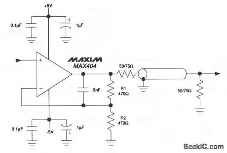
This circuit remains stable while driving unlimited capacitive video loads. As a result, flash A/D converter inputs, long-distance coaxial cables, and other larger or varying capacitive loads can be driven without output oscillation or ringing. Here, a MAX404 is connected as aback-terminated 50- or 75-Ω coax cable drive in a noninverting gain of 2,. Gain at the cable end is 1. (View)
View full Circuit Diagram | Comments | Reading(577)
Coaxial_line_driver
Published:2009/7/23 21:10:00 Author:Jessie
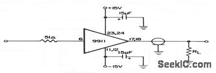
This circuit shows a 9911 used to drive long coaxial lines in a 50- or 75-Ω system, such as those found in test equipment and other applications. The 9911 is a high-current voltage follower and, in this application, is capable of driving long cables (and thus large capacitances) without instabilities. Remember that the 9911 provides 0.96 gain, which can drop to 0.90 when the chip is heavily loaded. RL should match the cable impedance (typically 50 or 75Ω). (View)
View full Circuit Diagram | Comments | Reading(581)
Wideband_amplifier_for_test_equipment_applications_high_gain
Published:2009/7/23 21:10:00 Author:Jessie
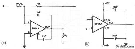
This circuit shows a 9914A used in an application where high speed at a relatively high gain is required (a gain of 100in this case). With the values given, this circuit can operate comfortably at frequencies of 20 MHz. If a lower gain is needed, connect a 1- to 5-pF capacitor between the output and inverting input to aid in suppressing parasitic oscillations. Figure 3-55B shows external connections for the 9914A. (View)
View full Circuit Diagram | Comments | Reading(621)
| Pages:47/126 At 204142434445464748495051525354555657585960Under 20 |
Circuit Categories
power supply circuit
Amplifier Circuit
Basic Circuit
LED and Light Circuit
Sensor Circuit
Signal Processing
Electrical Equipment Circuit
Control Circuit
Remote Control Circuit
A/D-D/A Converter Circuit
Audio Circuit
Measuring and Test Circuit
Communication Circuit
Computer-Related Circuit
555 Circuit
Automotive Circuit
Repairing Circuit