
Circuit Diagram
Index 997
SCHMITT_TRIGGER_AS_TIME_PROPORTIONING_TEMPERATURE_CONTROL
Published:2009/7/21 20:30:00 Author:Jessie
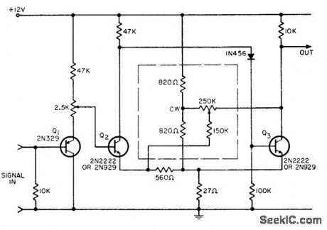
Hysteresis of Schmitt trigger (difference between turn-on und turnoff signal levels) is adjusted with negative feedback instead of positive, lo reduce hysteresis to less than 1 my. Trigger point can be adjusted above or below ground reference despite use of only one power supply. Modification of negative feedback causes dutycycle-controllable oscillation. Potentiometer adjusts circuit gain smoothly over wide range. -P. Lefferts, 'Super' Schmitt Uses Negative Feedback, EEE, 12:12, p 52-53. (View)
View full Circuit Diagram | Comments | Reading(921)
1_MHz_CRYSTAL_CALIBRATOR
Published:2009/7/21 20:30:00 Author:Jessie

Battery-powered crystal oscillator for checking frequency calibration of communication receiver uses TTL. Regulator is in TO-5 can, which is 100-mA version of LM309.-J. J. Carr, Resurrecting the Old War Horse: New Hope for the Old Receiver, Ham Radio, Dec. 1976, p 52-55. (View)
View full Circuit Diagram | Comments | Reading(1270)
NETWORK_TESTER
Published:2009/7/21 20:22:00 Author:Jessie

Sweep generator produces time-varying constant-amplitude frequency signal for network under test, with out-put of network converted to logarithmic DC voltage for display of amplitude or gain on decibel scale of CRO or recorder. Sawtooth voltage for sweep, generated by first Optical Electronics 3329 IC, drives another 3329 that converts sawtooth into logarithmic signal for log-frequency output. Detector uses 9004 absolute-value module as linear detector, with 2357 logamp converting output to decibel scale. Resulting display is Bode plot of frequency response.- A Simple Sweep Generator, Optical Electronics, Tucson, AZ, Application Tip 10201. (View)
View full Circuit Diagram | Comments | Reading(822)
UNIVERSAL_SIGNAL_GENERATOR
Published:2009/7/21 20:20:00 Author:Jessie

Collection of IC oscillators and dividers generates square waves from HF down to subaudible AF, along with markers up into VHF. Selectable oscillator section feeds fixed string of four divide-by-10 stages. Extra SN7490 divider can be switched in at various points along string to add divide-by-5 and divide-by-2 functions. LED in 1-MHz crystal stage indicates that circuit is oscillating. Second stage can be used with any external crystal up into low VHF range. Third stage accepts and conditions extemal sine or square input for feeding to divider chain. Extemal capacitor for fourth stage tunes square-wave generator from several hertz to several megahertz. Optional fifth stage is VCO for entire HF range up to 25 MHz.-J. Schultz, Updated Universal Frequency Generator, 73 Magazine, Nov. 1976, p 50-52. (View)
View full Circuit Diagram | Comments | Reading(1368)
SHORT_CIRCUIT_PROTECTION
Published:2009/7/21 11:06:00 Author:Jessie
Voltage-sensing short-circuit switch Q4-Q5 turns off series-regulating tronsistor Q1 when load R1 is short-circuited.-G. A. Chunn and G. D. Norton, Short-Circuit Protection Consumes Little Power, Electronics, 38:22, p 68. (View)
View full Circuit Diagram | Comments | Reading(0)
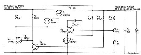
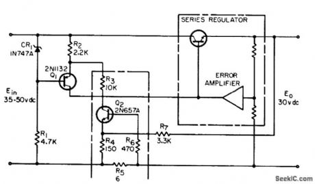
SERIES_REGULATOR_WITH_CAPACITIVE_OVER_LOAD_PROTECTION
Published:2009/7/21 11:04:00 Author:Jessie
R-C delaying network in dotted box applies drive slowly to series. pass transistor to prevent overload protective circuit from turning off regulator when surge current charges capacitive load. Network does not reduce response time.-J. Takesuye and H. Weber, Silicon Power Transistors Provide New Solutions to Voltage Control Problems, Motorola Application Note AN-163, Aug. 1964. (View)
View full Circuit Diagram | Comments | Reading(616)
HIGH_LOW_LEVEL_COMPARATOR_WITH_ONE_OP_AMP
Published:2009/7/7 4:00:00 Author:May
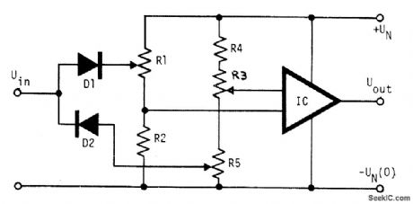
The voltage to be compared is fed through diode D1 and D2 to the voltage dividers R1 and R5 where the low and high limits are present. When the voltage level of an input signal exceeds the high threshold limit set with potentiometer R1, the diode D1 becomes forward biased and the increased voltage on the inputs of the op amp drives it into positive saturation. Similarly, a decrease of the input voltage at the op amp inputs turns the op amp to positive saturation. Potentiometer R3 is used for zeroing the op amp in the off state. (View)
View full Circuit Diagram | Comments | Reading(729)
COMPARATOR_DETECTS_POWER_SUPPLY_OVERVOLTAGES,CATCHES_GLITCHES
Published:2009/7/7 3:59:00 Author:May
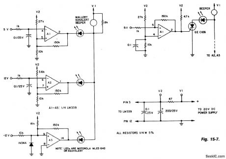
(A) To maintain an alarm condition when an overvoltage transient disappears, add an SCR to the comparator circuits. For SCR operation, voltages to the comparator inputs are inverted. (B) The triple-voltage monitoring circuit detects transient power-supply overvoltages. If excessive voltage momentarily appears at the 5, 12 and -12 V inputs, the LED for that circuit lights and the beeper sounds for as long as the overvoltage lasts. (View)
View full Circuit Diagram | Comments | Reading(1783)
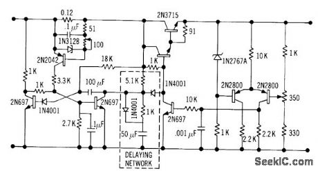
REDUCED_POWER_OVERLOAD_PROTECTION_
Published:2009/7/21 11:02:00 Author:Jessie
Circuit reduces power dissipotion in series regulator transistors under overload or short-circuit conditions by making output current decrease as load resistance decreases. Values shown are for 30 V d-c supply delivering 0.25 amp, with current limiting starting at 0.31 amp.-R. A. Lewis, Reduced-Power Overload Protection, EEE, 12:11, p 67. (View)
View full Circuit Diagram | Comments | Reading(685)
2_hp_THREE_PHASEINDUCTION
Published:2009/7/7 3:59:00 Author:May
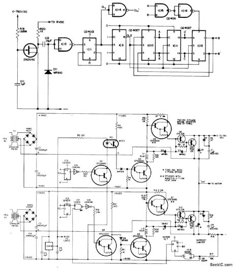
Speed is controlled by applying continuously variable DC voltage to VCO of control circuit for 750-VDC 7-A bridge inverter driving three sets of six Delco DTS-709 duolithic Darlingtons. Bridge inverter circuit for other two phases is identical to that shown for phase AA. VCO output is converted to three-phase frequency varying from 5 Hz at 50 VDC to 60 Hz at 600 VDC for driving output Darlingtons. Optoisolators are used for base drive of three switching elements connected to high-voltage side of inverter.- A 7A, 750 VDC Inverter for a 2 hp, 3 Phase, 480 VAC Induction Motor, Delco, Kokomo, IN, 1977, Application Note 60. (View)
View full Circuit Diagram | Comments | Reading(1499)
ADJUSTABLE_OVERLOAD_TRIP
Published:2009/7/21 11:01:00 Author:Jessie
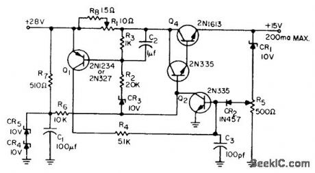
Protection circuit, added to conventional regulator, consists of R1, R2, R3, R4, C2, CR2, CR3, and Q1. When load current reaches preset trip level, drop across R1 tums on Q1, which in turn saturates Q2 ond cuts off regulator transistor Q3-Q4 to protect these transistors and reduce output voltage to zero. Turnoff is regenerative, hence fast. To reset, supply voltage is switched off and then back on.-W. A. O'Berry, Adjustable Overload Protection, EEE, 12:2, p 29. (View)
View full Circuit Diagram | Comments | Reading(608)
SHORT_PROOF_REGULATOR
Published:2009/7/21 11:00:00 Author:Jessie
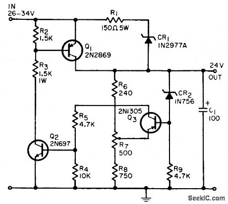
Provides constant 24 V at up to 500 ma and turns itself off when load is shorted. Restarts automatically when short is removed. Regulation is within 1% from no load to 500 ma and with input voltages from 26 to 34 V.-D. E. Wilson, Inexpensive Short-Proof Voltage Regulator, EEE, 12:6, p 64. (View)
View full Circuit Diagram | Comments | Reading(626)
TIMER_WITH_ALARM_
Published:2009/7/7 3:58:00 Author:May
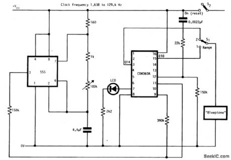
The circuit has two ranges: secs to 5 mins and 1 min to 80 mins.It can be powered by a 9-V battery.With the LED connected as shown a reasonable frequency of flashing occurs throughout the range of operation.This circuit is reset when S2 is closed. (View)
View full Circuit Diagram | Comments | Reading(745)
LOGIC_LINE_MONITOR
Published:2009/7/7 3:57:00 Author:May

This circuit requires only one CMOS IC, which is available in a 14-pin surface-mount package. The figure shows the logic lines going to a standard 9-bit parity comparator chip. This device is conventionally used in data transmission and recording applications to provide a means of error-detection by comparing the received eight- or nine-bit words with their corresponding parity bits. If the sum of the one's in a received word is odd but the odd-par-ity bit is low, then that word is known to be in error and requires retransmission.
When one of the logic lines decreases, the output of the parity comparator decreases, generating a wake-up interrupt to the microprocessor. The ninth line comes from a port on the microprocessor and is toggled to reset the output signal high again, ready for the next logic change.
(View)
View full Circuit Diagram | Comments | Reading(730)
LONG_TERM_ELECTRONIC_TIMER
Published:2009/7/7 3:57:00 Author:May
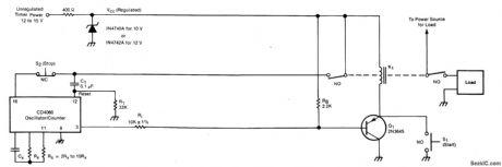
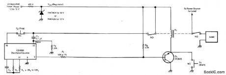
The timer includes an oscillator and a counter in an integrated circuit. The timing interval equals the oscillator period multiplied by the number of cycles to be counted.The oscillator frequency depends upon resistor RS and capacitor CX. The number of oscillator cycles to be counted before the counter output changes state is determined by the selection of the counter output terminal, shown here as pin 3. The interval can be set anywhere in the range from fractions of a second to months; it is given by T = 0.55 RSCX2n, where n is an integer determined by the counter-output selection.Operation is initiated by the closure of momentary switch S1 (or by a command signal having a similar effect). This grounds one side of relay K1, thereby activating the relay and causing the closure of the switches that supply power to the timer and to the load.The turn-on of VCC at the timer is coupled through C1 to the counter-reset terminal, thus resetting the counter. The initial reset voltage transient is then drained away through R1 to permit normal operation. During the first half cycle of the counter operation, the counter output voltage (at pin 3 in this case) is low. This tums on transistor Q1 so that relay K1 latches on, enabling the timer to continue running even though switch S1 has opened. The oscillator runs while the relay is on. When the number of oscillator cycles reaches the limit, the counter output voltage at pin 3 goes high. This tums off Q1, thereby tuming off the relay and returning the system to the original power-off state to await the next starting command. The timing cycle can also be interrupted and the system tumed off by opening normally-closed switch S2. (View)
View full Circuit Diagram | Comments | Reading(879)
WINDOW_COMPARATOR
Published:2009/7/7 3:56:00 Author:May
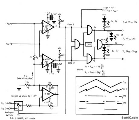
This circuit provides independently adjustable upper and lower threshold settings, and has sign, in window range, in upper window, and in lower window digital outputs. (View)
View full Circuit Diagram | Comments | Reading(0)
TRANSISTOR_THERMOMETER
Published:2009/7/21 21:21:00 Author:Jessie
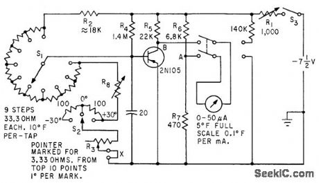
Base bias of germanium transistor varies linearly with temperature over wide ranee, at about 0.0014 v d-c per deg F. Meter is connected to measure base bias and calibrated in degrees for household and outdoor tempera tures. Range switch S1 covers 0 to 100°F in ten steps, and S2 extends range 30°in both directions.-L. E. Barton, Measuring Temperature with Diodes and Transistors, Electronics, 35:18, p 38-40. (View)
View full Circuit Diagram | Comments | Reading(662)
CYRO__TEMPERATURE__CONTROL
Published:2009/7/21 21:19:00 Author:Jessie
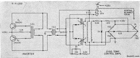
Regulates temperature to 0.5°F by sensing differences between gyro-mounted temperature-sensitive resistor R1 and fixed resistor R2 in bridge. Magnetic amplifier for bridge operates relay K1 to energize gyro heater when temperature is low, -R. E, King and H. Low, Solid-State Guidance For Able-Series Rockets, Electronics, 33:5, p 60-63. (View)
View full Circuit Diagram | Comments | Reading(608)
LONG_DELAY_LINE_FOR_LOGIC_SIGNALS
Published:2009/7/7 3:55:00 Author:May
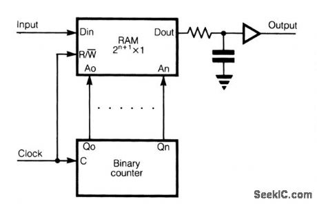

An extremely long delay of logic signal can be accomplished with this circuit. The logic signals to be delayed are applied to the,DIN of RAM. Address lines Ao,A1, . An are connected to outputs Qo, Q1, …… Qn of a binary counter. Clock input of counter and R/W input of RAM are joined together. However, it is sometimes necessary to put an inverter between those inputs, depending on the RAM and counter employed in line. In the first half of clock interval, content on outputs of counter is increased for 1 and content of chosen memory cell is read; in the second half of the clock interval, new content from DIN in the same memory cell is written. When full cycles of counting reaches the same memory cell, again we can read, in the first half of the clock interval of the following counting cycles, the chosen content. Delay time is:
Td=2 n+1·tcl
If clock frequency is not a multiple of input signal frequency, distortion of input signal is proportioned to the clock period. But if the clock frequency is a multiple of input signal frequency, there is no distortion. If we use RAM organized according to 2n+1 x 4 with separated data inputs and data outputs, we can have four parallel long delay lines. The resistor, capacitor, and buffer on DOUT of RAM are used to save output signal in writing time, when output of RAM becomes high impedance. (View)
View full Circuit Diagram | Comments | Reading(677)
001℃_DIFFERENTIAL
Published:2009/7/21 20:42:00 Author:Jessie
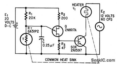
Scr conducts until heater reaches desired temperature, when thermistor T turns off unijunction oscillator Q.-R. G. Ferric, Thermostat Operates With 0.01℃ Differential, Electronics, 37:26, p 65. (View)
View full Circuit Diagram | Comments | Reading(476)
| Pages:997/2234 At 209819829839849859869879889899909919929939949959969979989991000Under 20 |
Circuit Categories
power supply circuit
Amplifier Circuit
Basic Circuit
LED and Light Circuit
Sensor Circuit
Signal Processing
Electrical Equipment Circuit
Control Circuit
Remote Control Circuit
A/D-D/A Converter Circuit
Audio Circuit
Measuring and Test Circuit
Communication Circuit
Computer-Related Circuit
555 Circuit
Automotive Circuit
Repairing Circuit