
Circuit Diagram
Index 993
RMS_TO_DC
Published:2009/7/7 4:51:00 Author:May
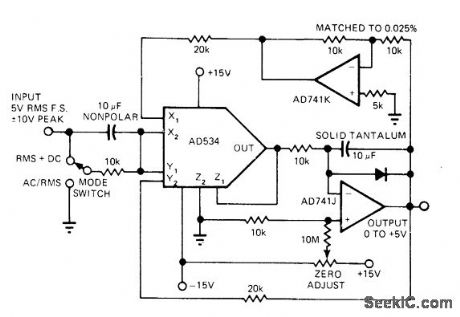
Single AD534 analog multiplier and two opamps compute RMS value of input signal as square root of sum of squares. Input is first squared at X2 and Y1 then time-averaged by integrator. Closing output loop back to X1 and Y2 completes square-rooting function. Crest factors up to 10 do not appreciably affect accuracy as long as input limits of multiplier are not exceeded. Accuracy is maintained up to 100 kHz. Article gives calibration procedure.-R. Frantz, Analog Multipliers-New IC Versions Manipulate Real-World Phenomena with Ease, EDN Magazine, Sept. 5, 1977, p 125-129. (View)
View full Circuit Diagram | Comments | Reading(1007)
420_450_MHz_100_W_LINEAR
Published:2009/7/7 4:50:00 Author:May
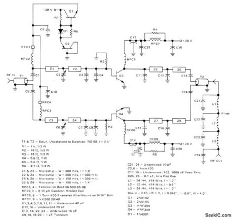
Two Motorola 3-inch lengths and prepare MRF309 transistors in pusffipull require only 16 and W drive to deliver 100 W for transmitter applications. Circuit provides 8 dB of power gain at efficiency greater than 40% when operating from 28-V supply. Harmonic suppression inherent in push-pull operation is enhanced by seven-element low-pass filter at output. Q1and Q2 are bias resistors and must be insulated from heatsink with mica washers. T1 and T2 are transformers constructed from RG58 coax. Use 1/4 inch at each end to give total transformer length of 21h inches.H. Swanson and B. Tekniepe, A 100-Watt PEP420-450 MHz Push-Pull Linear Amplifier, Motorola, Phoenix, AZ, 1978, EB-67. (View)
View full Circuit Diagram | Comments | Reading(732)
2_MHz_MASTER_CLOCK
Published:2009/7/7 4:47:00 Author:May
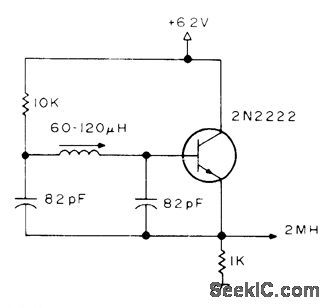


Developed for use with Geneml lnstruments AY-3-8500-1TV game chip,which contains dividers that deliver required 60-Hz vertical and 15.75-kHz horizontal sync signals for video signal going to TV set. Coil is Miller 9055 miniature slugtuned. Article gives other circuits for game.-S.Ciarcia,Hey,Look What My Daddy Builtl,73 Magazine,0ct.1976,p 104-108 (View)
View full Circuit Diagram | Comments | Reading(1004)
DIFFERENTIAL_TO_ABSOLUTE_VALUE
Published:2009/7/7 4:47:00 Author:May
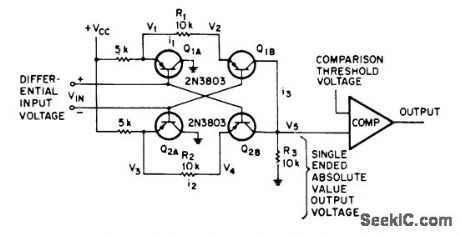
Used in comparing differential level to threshold level with good common-mode rejection. Input impedance is maintained high to avoid over loading differential input. Output voltage re-mains positive when input polarity is re-versed.-R. L. Wiker, Differential to Absolute Value Converter, EEE Magazine, Jan. 1971, p 65. (View)
View full Circuit Diagram | Comments | Reading(708)
143_156_MHz_80_W_AMPLIFIER
Published:2009/7/7 4:47:00 Author:May

Single transistor mounted on heavy heatsink provides about 9.4-dB gain. 8-W drive at 13.5 VDC produces full output power. Series tuning inductors are printed striplines with ground plane removed beneath them; report gives designs for photomasks. Transistor will withstand 20:1 VSWR at all phase angles,-T. Bishop, A Single-Device, 80-Watt, 50-Ohm VHF Amplifier, Motorola, Phoenix, AZ, 1978, EB-46. (View)
View full Circuit Diagram | Comments | Reading(1622)
OPTICALLY_COUPLED_V_F
Published:2009/7/7 4:44:00 Author:May
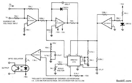
Input voltage range of 0-10 V is converted to proportional frequency at output of optoisolator with high linearitv bv RM4151 converter used in combination with RC3403A quad opamp that provides. functions of inverter, integrator, regulator, and LED driver.-"Linear Integrated circuit Data Book,"Raytheon Semiconductor Division, Mountain View,CA,1978, p 7-40-7-41. (View)
View full Circuit Diagram | Comments | Reading(610)
STALLED_MOTOR_PROTECTION
Published:2009/7/7 4:42:00 Author:May

Modification of basic speed control circuit for small DC permanent-magnet motors provides maximum current limit under normal conditions and reduced current limit under stall conditions, to limit dissipation of series transistor Q4, to safe value. When motor stalls, motor voltage falls, reducing voltage and motor current required to turn on Q3 and thereby limiting stalled-motor current,-D. Zinder, Current Limit and Foldback for Small Motor Control, EDN Magazine. May 5, 1974, p 77 and 79. (View)
View full Circuit Diagram | Comments | Reading(2425)
7_SEGMENT_TO_BCD_1
Published:2009/7/7 4:41:00 Author:May
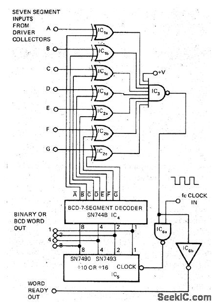
Arrangement uses SN7448 BCD to 7-segment decoder IC4.as lookup table for inverse decoding technique,When desired 7-segment code is applied to input of decoder and does not match output code from IC4.gate IC3,output is logic 1 This allows pulses from clock to advance BCD counter IC5,until its decoded state from IC4 matches that of input code,With coincidence,output of IC3 goes low, holding proper BCD code in IC5,and indicating by means of IC6b that BCD information is ready With 100-kHz clock,correct code is available for at least 90% of digit display time.-J.P.Cater,7-Segment to BCD Decoder,EDN Magazine,Feb.20,1973,p 92-93. (View)
View full Circuit Diagram | Comments | Reading(3326)
ISOLATED_15_V_DC_DC_CONVERTER
Published:2009/7/7 4:40:00 Author:May

In this circuit, a TL431 shunt regulator is used to sense the output voltage. The TL431 drives the LED of a 4N28 optocoupler which provides feedback to the MAX641 while maintaining isolation between the input, + 12 V, and the output, + 15 V. In this circuit, the + 15 V output is fully regulated with respect to both line and load changes.
(View)
View full Circuit Diagram | Comments | Reading(3024)
24_VDC_PROPORTIONAL_SPEED_CONTROL
Published:2009/7/7 4:39:00 Author:May
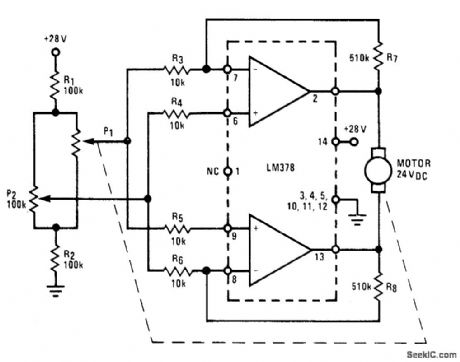
National LM378 amplifier IC is basis for low-cost proportional speed controller capable of furnishing 700 mA continuously for such applications as antenna rotors and motor-controlled valves. Proportional control results from error signal developed across Wheatstone bridge R1-R2-P1-P2. P1 is mechanically coupled to motor shaft as continuously variable feedback sensor. As motor turns, P1 tracks movement and error signal becomes smaller and smaller; system stops when error voltage reaches 0 V.- Audio Handbook, National Semiconductor, Santa Clara, CA, 1977, p 4-8-4-20. (View)
View full Circuit Diagram | Comments | Reading(2030)
SHORTWAVE_CONVERTER
Published:2009/7/7 4:38:00 Author:May

The NE602, U1, contains oscillator and mixer stages. The mixer combines the oscillator signal with the input rf signal to produce signals whose frequencies are the sum and difference of the input frequencies. For example, a 7.5-MHz signal is picked up by the antenna and mixes with the 8.5-MHz oscillator frequency. The difference between those two signals is 1 MHz-right in the center of your AM dial. Trans-former T1 is a 10.7-MHz i-f transformer. (View)
View full Circuit Diagram | Comments | Reading(958)
SQUARE_TO_SlNE
Published:2009/7/7 4:37:00 Author:May
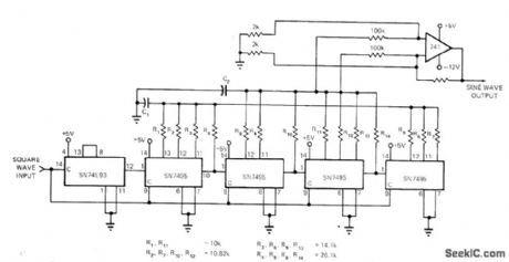
Transversal digital filter suppresses harmonics present on input square wave, to give pure sine wave. Resistors weight data as it passes through 16-bit shift register, so sine wave is sampled at 16 times its frequency and theoretically has no harmonics below the 16th. Simple RC filter removes remaining harmonics. Input is clock whose repetition rate is 16 times desired frequency. SN74L93 4-bit ripple counter divides this down to provide square wave of desired frequency. Square wave is sampled 16 times per cycle and shifted down SN7495 16-bit shift register. C1 and C2 are selected to eliminate higher harmonics. Sine-wave output has harmonic distortion of less than -50 dB.-L. J. Mandell, Sine-Wave
Synthesizer Has Low Harmonic Distortion, EDN Magazine, Aug. 15, 1972, p 52. (View)
View full Circuit Diagram | Comments | Reading(1244)
TRANSISTOR_PROTECTION_IN_MONO
Published:2009/7/21 10:27:00 Author:Jessie
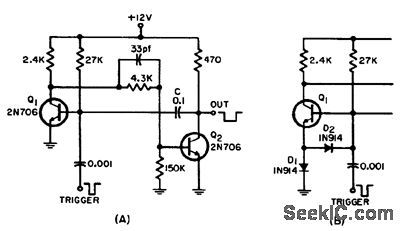
In typical transistor monostable mvbr (A), transient base-to-emitter voltage caused by discharging C often surpasses transistor rating. Two diodes alleviate trouble (B). Circuit produces width of 200 microsec.-J. S. Mikuckis, Base-Emitter Protection in Monostable Multivibrators, EEE, 12:9, p 63. (View)
View full Circuit Diagram | Comments | Reading(1014)
OVERLOAD_PROTECTION_WITH_TD
Published:2009/7/21 10:26:00 Author:Jessie

Tunnel diode-transistor level detector reduces load current of series voltage regulator to zero when preset limit is exceeded. Protective circuitry consists of TD1, PL1, R2, R3, Q3, and Q4.-G. E. Bloom, Overload Protection with a Tunnel Diode, EEE, 12:10, p 60 and 75. (View)
View full Circuit Diagram | Comments | Reading(625)
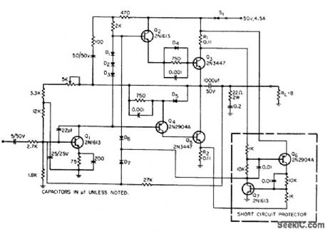
COMPLETE_GTO_PROTECTION_FOR_D_C_SUPPLY
Published:2009/7/21 10:24:00 Author:Jessie
Circuit includes required recycle pulse generator and Schmitt trigger for driving gate-turnoff scr (gto) that switches off d-c power supply within 30 microsec of over-load. Series regulator can deliver 125 V at 1 amp for input of 31 to 42 V. Overload trip point can be set anywhere between 0.75 and 1.2 amp. –W. C. Mosley, GTO Protection Circuitry for DC Supplies, EEE, 12:11, p 57-59. (View)
View full Circuit Diagram | Comments | Reading(950)
SHORT_CIRCUITABLE_30_W_AUDIO_AMPLIFIER_
Published:2009/7/21 10:21:00 Author:Jessie
Utilizes practically entire supply voltage to produce usable power output, provides fail-safe overload protection, and stabilizes bias current. Any temporary overload or current surge will turn off drive to output stage. Circuit must be reset manually, by turning S1 off, removing cause of overload, and turning S1 on again. Circuit will limit peak current in output transistors Q3 and Q5 to about 5 amp.-W. O. Hamlin, Transformer. less Amplifier with Overload Protection, EEE, 12:9, p 42-44. (View)
View full Circuit Diagram | Comments | Reading(1069)
POWER_SUPPLY_OVERLOAD_PROTECIION
Published:2009/7/21 10:20:00 Author:Jessie

Circuit uses simple relay instead of customary transistor to break load current when over-load or overvoltage occurs.-J. J. Rado, Versatile SCR Protection for Power Supplies, EEE, 13:8, p 56-62. (View)
View full Circuit Diagram | Comments | Reading(646)
4_18MHZ_CONVERTER
Published:2009/7/7 4:37:00 Author:May

The unit consists of rf amplifier Q1, local oscillator Q2, and mixer Q3. The two bands are covered without a bandswitch by using an i-f or 3.5 MHz. The oscillator range is 7.5 to 14.5 MHz. Incoming signals from 4 to 11 MHz are mixed with the oscillator to produce the 3.5-MHz i-f. Signals from 11 to 18 MHz are mixed with the oscillator to also produce an i-f of 3.5 MHz. At any one oscillator frequency, the two incoming signals are 7 MHz apart. Rf amplifier input C1/L1 comprises a high-Q, lightly loaded, tuned circuit; this is essential for good band separation. (View)
View full Circuit Diagram | Comments | Reading(1062)
OVERLOAD_PROTECTION_1
Published:2009/7/21 10:17:00 Author:Jessie
Series regulator with degenerative feedback provides both overload and short-circuit protection. Output voltage is automatically restored when over load is removed.-M. A. Torla, Series Regulator Gives Overload Protection, Electronics, 39:15, p 104-105. (View)
View full Circuit Diagram | Comments | Reading(1188)
VOLTAGE_TO_CURRENT
Published:2009/7/7 4:34:00 Author:May

Circuit is capable of supplying constant alternating current up to 1 A to variable load. Actual value of load current is determined by input voltage, values of R1-R3, and value of R5. Input of 250 mV gives 0.5 A through load (RMS values) with less than 0.5% total harmonic distortion. Applications include control of electromagnet current.- Audio Handbook, National Semiconductor, Santa Clara,CA,1977, p 4-21-4-28. (View)
View full Circuit Diagram | Comments | Reading(829)
| Pages:993/2234 At 209819829839849859869879889899909919929939949959969979989991000Under 20 |
Circuit Categories
power supply circuit
Amplifier Circuit
Basic Circuit
LED and Light Circuit
Sensor Circuit
Signal Processing
Electrical Equipment Circuit
Control Circuit
Remote Control Circuit
A/D-D/A Converter Circuit
Audio Circuit
Measuring and Test Circuit
Communication Circuit
Computer-Related Circuit
555 Circuit
Automotive Circuit
Repairing Circuit