
Circuit Diagram
Index 985
Full_range_AC_power_control_circuit_using_a_triac
Published:2009/7/21 8:05:00 Author:Jessie
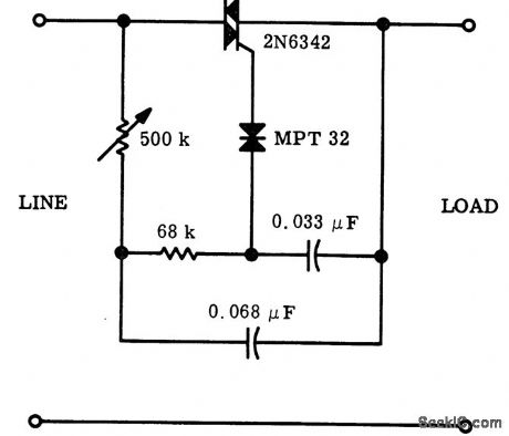
Full range AC power control circuit using a triac (courtesy Motorola Semiconductor Products Inc.). (View)
View full Circuit Diagram | Comments | Reading(1729)
WIDEBAND_500_kHz_1_GHz_HYBRID_AMPLIFIER
Published:2009/7/7 7:57:00 Author:May
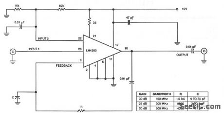
The amplifier's input stageis a dual-gate GaAs FET, which provides low mput capacitance and hightransconductance. The dual-gate structure accepts the signal on mput 1. Input 2 controls the gain of theamplifier. The amplifier has a third input for use h senes feedback. The output feeds back to pm 3 via asingle resistor, which controls the overall power galn of the ampllfter. At 10 MHz, the output is capable ofdelivering 12 dBm into a 50-Ω load with 1 dB of signal compression. The accoupled amplifier has a gam of 37 dB at 100 MHz and 3 dB at 1 GHz. (View)
View full Circuit Diagram | Comments | Reading(708)
PNPN_ONE_SHOT
Published:2009/7/21 8:04:00 Author:Jessie
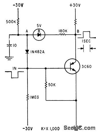
Provides up to 10 sec delay. Circuit is normally on, with point A at -11 v and B at +1 v. Negative trigger op plied to base of pnpn unit operates circuit.-J. B. Hangstefer and L. H. Dixon, Jr., Triggered Bistable Semiconductor Circuits, Electronics, 32:35, p 58-60. (View)
View full Circuit Diagram | Comments | Reading(675)
MINIATURE_WIDEbAND_AMPLIFIER
Published:2009/7/7 7:53:00 Author:May
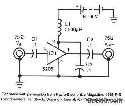
This wideband amplifier uses only five compo-nents. External signals enter pin 3 of IC1 via ac coupling capacitor C1. Following amplification, the boosted signals from IC1 pin 1 are coupled to the output by capacitor C2. Capacitor C3 decouples the dc power supply, while rf current is isolated from the power supply by rf choke L1.The NE5205's low current consumption of 25 mA at 6 Vdc makes battery-powered operation a reality. Although the device is rated for a 6 to 8 V power supply, 6 V is recommended for normal operation. From 6 V an internal bias of 3.3 V results, which permits a 1.4 V pk-pk output swing for video applications. (View)
View full Circuit Diagram | Comments | Reading(0)
100_MHz_VHF_CRYSTAL_OSCILLATOR
Published:2009/7/7 7:53:00 Author:May

Figure 21-13 shows a 100-MHz oscillator operating on the fifth harmonic. Again to maintain the transistor's gain, note the increase in the collector's load resistance R1 because of the increase in the quartz crystal's internal series resistance Rs. C3 is needed at frequencies above 50 MHz to tune out the shunting effect of L1 on R1, to maintain a high load resistance for the transistor and get enough gain for oscillation.The equivalent series RLCL load across the crystal is 8.2 Ω (RL) and 200 pF (CL).
(View)
View full Circuit Diagram | Comments | Reading(1816)
Direction_and_speed_control_for_shunt_wound_motors
Published:2009/7/21 8:04:00 Author:Jessie
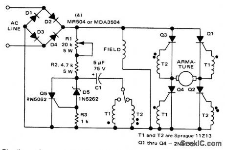
Direction and speed control for shunt-wound motors (courtesy Motorola Semiconductor Products Inc.). (View)
View full Circuit Diagram | Comments | Reading(1637)
MARKER_GENERATOR
Published:2009/7/7 7:50:00 Author:May
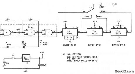
The oscillator section uses three sections of a 7400 quad NAND gate integrated circuit. The 1-MHz signal from the oscillator is fed into a 7490 decade counter configured to divide by ten, providing the 100-kHz signal. To obtain the 50 and 25 kHz outputs, the 100-kHz signal is further divided by 7473 dual J-K flip-flop. The first half of the 7473 divides the 100-kHz signal by two, yielding the 50 kHz signal. The second half of the 7473 again divides by two, giving the 25 kHz signal. S2 selects the output, a square wave, rich in harmonics. The generator can be powered from any convenient 6 to 12 Vdc source. A 7805 ftxed-voltage regulator supplies the regulated voltage for the oscillator and the divider chips. The generator described here is powered by a 9-V transistor radio battery. (View)
View full Circuit Diagram | Comments | Reading(2043)
BROADCAST_BAND_RF_AMPLIFIER
Published:2009/7/7 7:50:00 Author:May

The circuit has a frequency response ranging from 100 Hz to 3 MHz;gam is about 30 dB,Field-effecttransistor Q1is configured In the coΠ1mon-source self-biased mode. Optional resistor R1 allows you to setthe input impedance to any desired value;commonly,it will be 50 Ω.The signalis then direct coupled to Q2, a common-base circuit that isolates the input and outputstages and provides the amplifier’s exceptional stability. Last, Q3 functions as an emitter follower, to provide low output impedance at about 50 Ω.If you need higher output impedance,include resistor R8. It willaffect impedance according to this formula:R8≈ROUT -50. Otherwise,connect output capacitor C4directly to the emitter of Q3. (View)
View full Circuit Diagram | Comments | Reading(3128)
20_MHz_VHF_CRYSTAL_OSCILLATOR
Published:2009/7/7 7:47:00 Author:May

A typical circuit at 20 MHz is shown. The crystal, which has an internal series resistance RS, of 14 Ω , oscillates at its third harmonic. The diode clamp D1 and D2 provides a constant amplitude control. The transistor operates continuously in a linear mode over a complete cycle of oscillation, and reflects a reasonably constant load across the crystal at an times. (View)
View full Circuit Diagram | Comments | Reading(693)
WIDEBAND_UHF_AMPLIFIER_WITH_HIGH_PERFORMANCE_FETS
Published:2009/7/7 7:46:00 Author:May
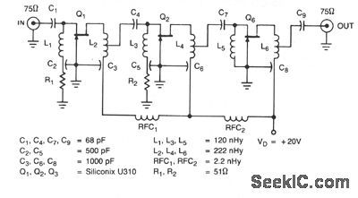
The amplifier circuit is designed for a 225 MHz center frequency, 1 dB bandwidth of 50 MHz, low-input VSWR in a 75-Ω system, and 24 dB gain. Three stages of U310 FETs are used, in a straight-forward design. (View)
View full Circuit Diagram | Comments | Reading(0)
28_dB_NONINVERTING_AMPLIFIER
Published:2009/7/7 7:42:00 Author:May
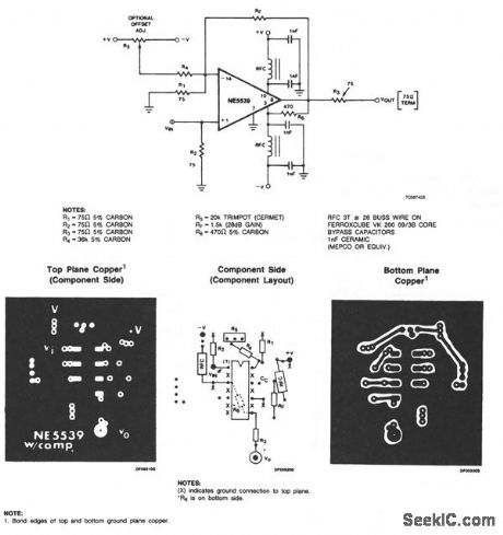
The physical circuit layout is extremely critical. Breadboarding is not recommended. A double-sided copper-clad printed circuit board will result in more favorable system operation. (View)
View full Circuit Diagram | Comments | Reading(518)
29_MHz_AMPLIFIER
Published:2009/7/7 7:40:00 Author:May
The only adjustments that require close attention are input, output, and neutralization. The 150-pF capacitor in the input line compensates for impedance mismatch. You tune for maximum signal transfer from exiter to final with an in-line meter or external field strength meter. The final is a conventional pi network. When neutralized, the plate current dip should be at about the same setting of the 20-pF plate capacitor as maximum output. Adjust bias to let tubes idle at about 30 mA. (View)
View full Circuit Diagram | Comments | Reading(566)
MOS_48_based_analog_processor
Published:2009/7/21 8:19:00 Author:Jessie

MOS-48 based analog processor. This circuit shows the MP-10 D/A convener and the MP-20 A/D convener connected to the 8748 processor (courtesy Intel Corporation). (View)
View full Circuit Diagram | Comments | Reading(1034)
TV_vertical_sync_delay_circuit
Published:2009/7/21 8:18:00 Author:Jessie

TV vertical sync delay circuit (courtesy Motorola Semiconductor Products Inc) (View)
View full Circuit Diagram | Comments | Reading(909)
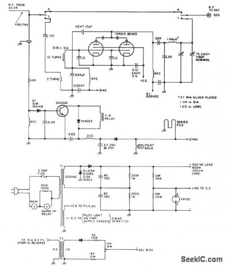
80_W_PEP_3_30_MHz_125_136_V_AMPLIFIER
Published:2009/7/7 7:39:00 Author:May
This amplifier utilizes a 2N6367 and a pair of 2N6368 transistors. The 2N6367 transistor is employed as a driver and is specified for up to 9 W (PEP) output. In the amplifier design the driver must supply on 5 W (PEP) at 30 MHz with a resulting IMD performance of about -37 to -38 dB. At lower operating fre-quencies, drive requirements drop to the 2-3 W (PEP) range and IMD performance improves to better than 40 dB. Two 2N6368 transistors are employed in the final stage of the transmitter design in a push-pull configuration. These devices are rated at 40 MI (PEP) and -30 dB maximum IMD, although -35 dB per-formance is more typical for narrowband operation. Without frequency compensation, the completed amplifier can deliver 90W (PEP) in the 25-30 MHz band with IMD performance down -30 dB. If only the power amplifier stage is frequency compensated, 95 W (PEP) can be obtained at 6- 10 MHz. (View)
View full Circuit Diagram | Comments | Reading(1077)
Memory_mapped_output_device_interfaced_with_the_MCS_80_8080A_CPU_system
Published:2009/7/21 8:16:00 Author:Jessie

Memory mapped output device interfaced with the MCS-80 (8080A) CPU system (courtesy Analog Devices, Inc.). (View)
View full Circuit Diagram | Comments | Reading(651)
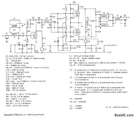
2_30_MHz_140_W_PEP_AMATEUR_RADIO_LINEAR_AMPLIFIER
Published:2009/7/7 7:36:00 Author:May

He amplifier operates across the 2-30 MHz band with relatively flat gain response and reaches gain saturation at approximately 210 W of output power. Both input and output transformers are 4:1 turns ratio (16:1 impedance ratio) to achieve low input SWR across the specified band and a high saturation capability.When using this design, it is important to interconnect the ground plane on the bottom of the board to the top, especially at the emitters of the MRF454s. (View)
View full Circuit Diagram | Comments | Reading(669)
HALL_EFFECT_COMPASS
Published:2009/7/7 7:32:00 Author:May
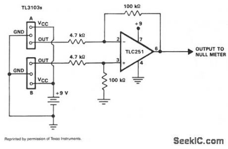
The TL3103 linear Hall-effect device can be used as a compass. By definition, the north pole of a magnet is the pole that is attracted by the mag-netic north pole of the earth. The north pole of a magnet repels the north-seeking pole of a compass. By convention, lines of flux emanate from the north pole of a magnet and enter the south pole, The cir-cuit of the compass is shown. By using two TL3103 devices instead of one, we achieve twice the sensitivity. With each device facing the opposite direc-tion, device A would have a position output while the output of device B would be negative with respect to the zero magnetic field level. This gives a differential signal to apply to the TLC251 op amp. The op amp is connected as a difference amplifier with a gain of 20. Its output is applied to a null meter or a bridge balance indicator circuit. (View)
View full Circuit Diagram | Comments | Reading(2136)
HALL_EFFECT_SWITCHES
Published:2009/7/7 7:31:00 Author:May
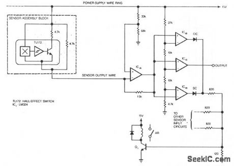
Hall-effect switches have several advantages over mechanical and optically coupled switches. They're insensitive to environmental light and dirt, they don't bind, and they don't sustain mechanical wear. Their major drawback is that they require three wires per device. The circuit shown, however, reduces this wire count to N + 1 wires for N devices.Amplifier IC1A is configured as a current-to-voltage converter. It senses the sensor assembly's out-put current. When the Hall-effect switch is actuated, the sensor's output current increases to twice its quiescent value. Amplifier IC1B, configured as a comparator, detects this increase. The comparator's out-put decreases when the Hall-effect switch turns on.The circuit also contains a fault-detection function. If any sensor output wire is open, its correspond-ing LED will turn on. If the power-supply line opens, several LEDs will turn on. A short circuit will also turn an LED on. Every time an LED turns on, Q1 turns on and the alarm relay is actuated. (View)
View full Circuit Diagram | Comments | Reading(3479)
Full_wave_SCR_bridge_power_supply_for_cotor_TV_rated_at_80_volts_15_amperes
Published:2009/7/21 8:15:00 Author:Jessie

Full-wave SCR bridge power supply for cotor TV rated at 80 volts, 1.5 amperes. This circuit is designed for 19-inch color receivers (courtesy Motorola Semiconductor Products Inc.). (View)
View full Circuit Diagram | Comments | Reading(1841)
| Pages:985/2234 At 209819829839849859869879889899909919929939949959969979989991000Under 20 |
Circuit Categories
power supply circuit
Amplifier Circuit
Basic Circuit
LED and Light Circuit
Sensor Circuit
Signal Processing
Electrical Equipment Circuit
Control Circuit
Remote Control Circuit
A/D-D/A Converter Circuit
Audio Circuit
Measuring and Test Circuit
Communication Circuit
Computer-Related Circuit
555 Circuit
Automotive Circuit
Repairing Circuit