
Circuit Diagram
Index 988
12_GHz_FREQUENCY_COUNTER
Published:2009/7/7 6:38:00 Author:May

The output of the CA3179 is fed through the D1/Q1 circuit. Those components serve to boost the 1-V output of the CA3179 to a standard TTL level. Then, depending on the position of range switch S2b, the signal is passed directly to the 7216, or through the divide-by-four circuit built from the two D flip-flops in IC3.
The other half of the range switch S2a controls the voltage at pin 3 of the CA3179. When pin 3 is high, the signal applied to pin 9 is fed through an extra internal divide-by-four stage before it is amplified and output on pins 4 and 5. When pin 3 is low, the signal on pin 13 is simply processed for output without being divided internally.
A 3.90625-MHz crystal provides the time base; the crystal yields a fast gate time of 0.256 second.The displayed frequency equals the input frequency divided by 1000 in the fast mode. In slow mode, gate time is 2.56 seconds. The displayed frequency equals the input frequency divided by 100 in the slow mode.
Switch S4, gate time, performs two functions. First it selects the appropriate gate time according to which digit output of IC1 the range input is connected to. Another of the 7216's inputs is also contro0ed by S4: the dp select input. The decimal point of the digit output to which that pin is connected will be the one that lights up. The correct decimal point illuminates, according to the position of S4, to provide a reading in MHz.
(View)
View full Circuit Diagram | Comments | Reading(1818)
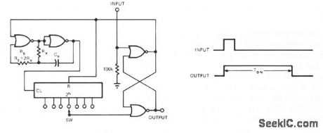
RETRIGGERABLE_ONE_SHOT
Published:2009/7/7 6:36:00 Author:May
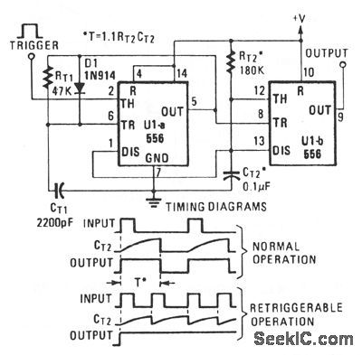
View full Circuit Diagram | Comments | Reading(503)
LOW_FREQUENCY_MULTIVIBRATOR
Published:2009/7/7 6:35:00 Author:May
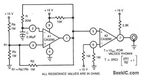
This circuit uses half the CA3290 BiMOS dual voltage comparator as conventional multivibrator. The second half maintains frequency against effects of output loading. Large values of timing resistor, R1, assure long time delays with low-leakage capacitors. (View)
View full Circuit Diagram | Comments | Reading(502)
LINEAR_RAMP_MONOSTABLE
Published:2009/7/7 6:34:00 Author:May
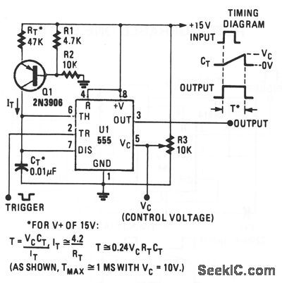
View full Circuit Diagram | Comments | Reading(455)
PROGRAMMABLE_FREQUENCY_ASTABLE
Published:2009/7/7 6:33:00 Author:May
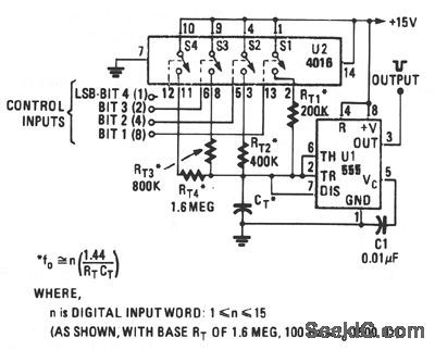
View full Circuit Diagram | Comments | Reading(1556)
FUNCTION_GENERATOR_1
Published:2009/7/7 6:32:00 Author:May

This generator will supply she, triangular, and square waves from 2 Hz to 20 kHz. This complete test instrument can be plugged into a standard 110 Vac line for power.VOUT will be up to ±25 V (50 V pk-pk across loads as small as 100 Ω about 2.5 A maximum output current).Capacitor working voltages should be greater than 50 Vdc and all resistors should be 1/2 W, unless otherwise indicated. The interconnecting leads from the 741 pins 2 and 3 to their respective resistors should be kept short, less than 2 inches if possible; longer leads might result in oscillation. Full output swing is possible to about 5 kHz; after that the output begins to taper off because of the slew rate of the 741, until at 20 kHz the output swing will be about 20Vpp ±10 V. This problem can be remedied by simply using an op amp with a higher slew rate, such as the LF356. (View)
View full Circuit Diagram | Comments | Reading(1717)
FREQUENCY_COUNTER_PREAMP
Published:2009/7/7 6:30:00 Author:May

By using the preamplifier with a short length of shielded cable and clip leads, signals that generally could not generate a readout, generate precise and stable readouts on the counter. The DPDT switch is used to bypass the circuit when amplification is not needed. The preamplifier can also be used for other purposes. For example, the unit was also tested as a receiver preamplifier and increased received signal strength about 6 S-units at 30 MHz. A line tap can be used to measure the frequency directly at the output of a transmitter. The entire circuit for that consists of two diodes, one resistor, and one capacitor. The line tap simply picks a low-amplitude signal for measurement by the frequency counter. The tap can be connected to transmitters with an output power of between 1 and 250 W. (View)
View full Circuit Diagram | Comments | Reading(3300)
PROGRAMMABLE_FREQUENCY_FREE_RUNNING_MULTIVIBRATOR
Published:2009/7/7 6:29:00 Author:May
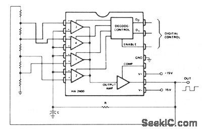
This is the simplest of any programmable oscillator circuit, since only one stable timing capacitor is required. The output square wave is about 25 V pk-pk, and has rise and fall times of about 0.5 μs. If a programmable attenuator circuit is placed between the output and the divider network, 16 frequencies can be produced with two HA-200's and still only one timing capacitor. (View)
View full Circuit Diagram | Comments | Reading(640)
MONOSTABLE_OPERATION
Published:2009/7/7 6:28:00 Author:May
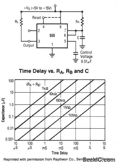
In this mode, the timer functions as a one shot. The external capacitor is initially held discharged by a transistor internal to the timer. Applying a negative trigger pulse to pin 2 sets the flip-flop, driving the output high, and releasing the short circuit across the external capacitor. The voltage across the capacitor increases with the time constant r = RAC to 2/3 VS, where the comparator resets the flip-flop and discharges the external capacitor. The output is now in the low state.Circuit triggering takes place when the negative-going trigger pulse reaches 1/3 VS; the circuit stays in the output high state until the set time elapses. The time the output remains in the high state is 1.1 RAC and can be determined by the graph. A negative pulse applied to pin 4 (reset) during the timing cycle will discharge the external capacitor and start the cycle over again beginning on the positive-going edge of the reset pulse. If reset function is not used, pin 4 should be connected to Vs to avoid false resetting. (View)
View full Circuit Diagram | Comments | Reading(519)
TRIANGLE_GENERATOR
Published:2009/7/7 6:25:00 Author:May

This circuit generates a symmetrical, 10-mV pk-pk triangle waveform which is summed with a dclevel and connected to the a/d analog input fornoise/DNL testing. The dc level input offsets thetriangle waveform over the input range of the ADC. The 10-mV amplitude amounts to an 8 LSB span for a 12-bit, 5-V. full-scale ADC. (View)
View full Circuit Diagram | Comments | Reading(682)
TWO_FUNCTION_SIGNAL_GENERATOR
Published:2009/7/7 6:24:00 Author:May

You can continously vary the frequencies of the triangle and square waves produced by this circuit over a full decade. If R5 = R3, the amplitude of the two waveforms will be equal (ASOUARE = ATRIANGLE). (View)
View full Circuit Diagram | Comments | Reading(547)
40_MHz_UNIVERSAL_COUNTER
Published:2009/7/7 6:21:00 Author:May

This circuit can be used to measure frequencies up to 40 MHz. To obtain the correct measured value, it is necessary to divide the oscillator frequency and the input frequency by four. In doing this, the time between measurements is also lengthened to 800 ms and the display multiplex rate is decreased to 125 Hz.
(View)
View full Circuit Diagram | Comments | Reading(1734)
ASTABLE
Published:2009/7/7 6:21:00 Author:May
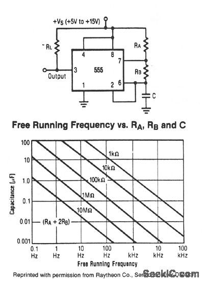

This astable will trigger itself and run free as a multivibrator. The external capacitor charges through RA and RB and discharges through RB only. Thus, the duty cycle is set by the ratio of these two resistors, and the capacitor charges and discharges between 1/3 VS and 2/3 VS. The charge and discharge times, and therefore frequency, are independent of supply voltage. The free-running frequency versus RA, RB and C is shown in the graph. (View)
View full Circuit Diagram | Comments | Reading(1094)
LOW_POWER_WIDE_RANGE_PROGRAMMABLE
Published:2009/7/7 6:19:00 Author:May
This CMOS circuit can be used as a 1-shot time delay switch and general-purpose timer. The circuit consists of a gated oscillator and a latch made from one CD4001 quad 2-input NOR gate as shown and a CD4020 14-stage counter. TON is a function of the oscillator frequency from the RxCx and the proper 2N output from the counter. A pulse applied to the latch will enable the oscillator and counter. The latch output will remain high until the 2N count resets the latch and disables the oscillator and counter. The circuit provides μs to hour interval timing. The extraordinarily long periods available from the CMOS oscillator, combined with the 14-stage counter, make this range possible. Further decoding is required for variations finer than a power of two. (View)
View full Circuit Diagram | Comments | Reading(630)
EASILY_TUNED_SINE_WAVE_SQUARE_WAVE_OSCILLATOR
Published:2009/7/7 6:18:00 Author:May

The circuit will provide both a sine- and square-wave output for frequencies from below 20 Hz to above 20 kHz. The frequency of oscillation is easily tuned by varying a single resistor. This is a considerable advantage over Wien-Bridge circuits where two elements must be tuned simultaneously to change frequency. Also, the output amplitude is relatively stable when the frequency is changed. An amp is used as a tuned circuit, driven by square wave from a voltage comparator. The frequency is controlled by R1, R2, C1, C2, and R3, with R3 used for tuning. Tuning the filter does not affect its gain or bandwidth, so the output amplitude does not change with frequency.A comparator is fed with the sine-wave output to obtain a square wave. The square wave is then fed back to the input of the tuned circuit to cause oscillation. Zener diode, D1, stabilizes the amplitude of the square wave fed back to the filter input. Starting is insured by R6 and C5 which provide dc negative feed-back around the comparator. This keeps the comparator in the active region. Distortion ranges between 0.75% and 2% depending on the setting of R3. Although greater tuning range can be accomplished by increasing the size of R3 beyond 1 KΩ, distortion becomes excessive. Decreasing R3 lower than 50 Ω can make the filter oscillate by itself. (View)
View full Circuit Diagram | Comments | Reading(805)
10_MHz_FREQUENCY_COUNTER
Published:2009/7/7 6:17:00 Author:May

The circuit consists of ICM7208 seven-decade counter U1, ICM7207A oscillator controller U2, and CA3130 biFET op amp U3. IC UI counts input signals, decodes them to 7-segment format, and outputs signals that are used to drive a 7-digit display. IC U2 provides the timing for U1, while U3 conditions the input to U1. The The circuit consists of ICM7208 seven-decade counter U1, ICM7207A oscillator controller U2, and CA3130 biFET op amp U3. IC U1counts input signals, decodes them to 7-segment format, and outputs signals that are used to drive a 7-digit display. IC U2 provides the timing for U1, while U3 conditions the input to U1. The 5.24288-MHz crystal frequency is divided by U2 to produce a 1280-MHz multiplexing signal at pin 12 of U2. That signal is input to U1 at pin 16 and used to scan the display digits in sequence.crystal frequency is divided by U2 to produce a 1280-MHz multiplexing signal at pin 12 of U2. That signal is input to U1 at pin 16 and used to scan the display digits in sequence. (View)
View full Circuit Diagram | Comments | Reading(0)
UP_DOWN_COUNTER_EXTREME_COUNT_FREEZER
Published:2009/7/7 6:12:00 Author:May
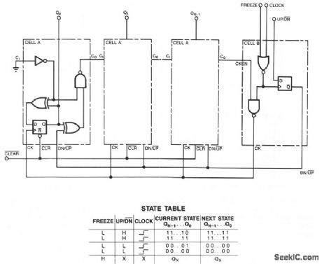
The discrete-gate up/down-counter design has the unusual property of freezing, or saturating, when it reaches its lowest count in the down-count mode or its highest count in the count-up mode instead of rolling over and resetting as do most counters. This property proves especially useful in position-control systems. For example, you wouldn't want a robot's arm to slowly move to full extension as the counter counts up and then have it suddenly slam back to its rest position when the counter resets to zero.
You can cascade as many of the A cells as you need because the counter's outputs are synchronous.The B cell accepts the carry bit from the most significant bit's A cell and provides the clock control that stops the counter. Make sure that the freeze input to the B cell doesn't get asserted when the clock input is low; otherwise, the counter might make an extra count.
(View)
View full Circuit Diagram | Comments | Reading(595)
LOW_COST_FREQUENCT_COUNTER
Published:2009/7/7 5:54:00 Author:May

This counter uses a four-digit display, but with a flip of the range switch, it can display frequencies from 1 to 40 MHz, with a resolution of 100 Hz. The MM74C926 CMOS IC contains a four-digit decimal counter that can latch a given count and then use this information to drive a 7-segment, common-cathode multiplexed (MUX) display. The block diagram and schematic show the operation of the counter. Crystal-controlled timer U1 through U3 produces a 5-Hz square wave used for timing the frequency count. Y1 is a TV color-burst crystal operating in a reliable circuit that controls the oscillator frequency. U1 acts as the oscillator and also divides the fundamental operating frequency of 3.579545 MHz to produce a square-wave output of 60 Hz. U2 divides the 60-Hz output of U1 by six. In turn, the 10-Hz output of U2 is divided by two in U3, a dual flip-flop, to produce the 5-Hz pulse.
A quad, two-input, Schmitt-triggered NAND U4 is used for gating the rf-signal input and for generating the counter control pulses-Section U4D is unused. The 5-Hz output pulse of U3 is applied to the rf-signal input gate at U4A pin 2. When the timer output signal is low, the gate is closed. (View)
View full Circuit Diagram | Comments | Reading(3564)
PULSE_TRAIN_TO_SINUSOID_CONVERTER
Published:2009/7/7 5:47:00 Author:May

The circuit lets you convert a serial pulse stream or sinusoidal input to a sinusoidal output at 1/32 the frequency. By varying the frequency of VIN, you can achieve an output range of 107:1-from about 100 kHz to less than 0.01 Hz. The output resembles that of a 5-bit d/a converter operating on parallel digital data.
Counter IC1 generates binary codes that repeatedly scan the range from 00000 to 11111. The output amplifier adds the corresponding XOR gate outputs, VDD or ground, weighted by the values of input resistors R1 through R4. The 16 counter codes 00000 to 01111, for instance, pass unchanged to the XOR gate outputs, and cause VOUT to step through the half-sinusoidal cycle for maximum amplitude to minimum amplitude.
Counter output Q4 becomes high for the next 16 codes, causing the XOR gates to invert the Q0 through Q3 outputs. As a result, VOUT steps through the remaining half cycle from minimum to maximum amplitude. The counter then rolls over and initiates the next cycle. You can change the RI through R4 values to obtain other VOUT waveforms. VDD should be at least 12 V to assure maximum-frequency operation from IC1 to IC2.
(View)
View full Circuit Diagram | Comments | Reading(867)
POWER_TRANSFORMER_SWITCHING_RELAY_SENSES_LINE_VOLTAGE
Published:2009/7/21 10:04:00 Author:Jessie
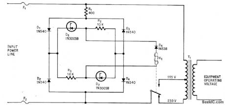
For 230-V line voltage, zener diodes back-bias D5, preventing energization of relay. For 115 V, diode conducts and relay closes, connecting line to 115-V tap of transformer. –L. K. Moyer, Circuit Always Applies Correct Operating Voltage, Electronics, 37:25, p 77. (View)
View full Circuit Diagram | Comments | Reading(787)
| Pages:988/2234 At 209819829839849859869879889899909919929939949959969979989991000Under 20 |
Circuit Categories
power supply circuit
Amplifier Circuit
Basic Circuit
LED and Light Circuit
Sensor Circuit
Signal Processing
Electrical Equipment Circuit
Control Circuit
Remote Control Circuit
A/D-D/A Converter Circuit
Audio Circuit
Measuring and Test Circuit
Communication Circuit
Computer-Related Circuit
555 Circuit
Automotive Circuit
Repairing Circuit