
Circuit Diagram
Index 995
400_CPS_SCR_REGULATED_SUPPLY
Published:2009/7/21 10:47:00 Author:Jessie
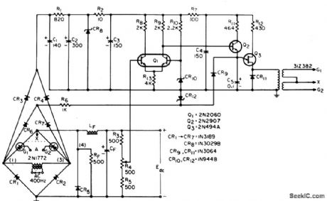
Converts 115 V at 400 cps to 24 V d-c, using ramp-and-pedestal control of ser firing. Regulation is excellent, ripple can be as small as desired, and sync circuit provides automatic short-circuit protection. Efficiency is 95% because power dissipation is low when scr's are not conducting. Either side of supply can be grounded.-G. B. Jordan,A Novel Sync Circuit for Scr Control, EEE, 14:7, p 58-61. (View)
View full Circuit Diagram | Comments | Reading(737)
LOW_DISSIPATION_TRANSISTOR_OVERVOLT_AGE_FUSE
Published:2009/7/21 10:45:00 Author:Jessie
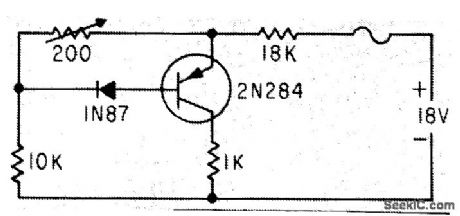
Series collector resistor lowers dissipation of fuse circuit during normal line voltages, and serves also as voltage regulator for transistors being protected (represented by 1K load).-K. Redmond, Low-Cost Transistor Overload Safety Circuit, Electronics, 33:42, p 102. (View)
View full Circuit Diagram | Comments | Reading(505)
PULSE_HEIGHT_TO_TIME
Published:2009/7/7 4:25:00 Author:May
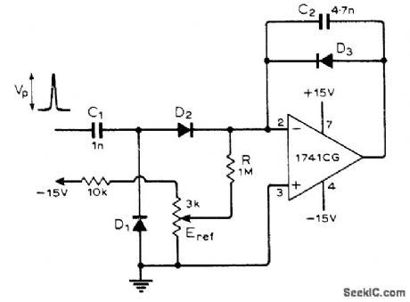
Simple opamp cir-cuit produces time interval proportional to height of positive input pulse, Opamp is con-nected as integrator whose output is held at about zero by negative feedback through D3. Positive input pulse charges C1 and C2, amplifier output steps down, and D3 is reverse-biased. Time for output to charge back up to zero, as observed on oscilloscope, is then directly proportional to input pulse height. Article gives de-sign equations.-G. B. Clayton, Experiments with Operational Amplifiers, Wireless World, Sept. 1973, p 447-448. (View)
View full Circuit Diagram | Comments | Reading(520)
BATTERY_STANDBY
Published:2009/7/21 10:44:00 Author:Jessie
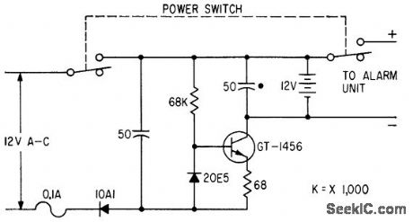
Protects against false alarms caused by power failure of intruder detector.-S. M. Bogno, Sensitive Capacitance Intruder Alarm, Electronics, 33:38, p 65-67. (View)
View full Circuit Diagram | Comments | Reading(550)
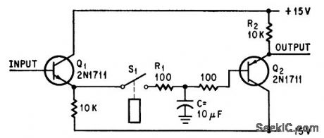
OVERLOAD_PROTECTION_2
Published:2009/7/21 10:42:00 Author:Jessie

Switches power off rapidly to prevent current overloads from damaging transistors in breadboard circuits under test. Voltage drop across 0.47-ohm resistor and Q1 biases Q2 to saturation, causing Q3 and Q4 to open power relay.- F. W. Kear, Laboratory Supply for Transistors, Electronics, 35:30, p 55-57. (View)
View full Circuit Diagram | Comments | Reading(570)
PULSED_TRANSDUCER_METER_PROTECTION
Published:2009/7/21 10:41:00 Author:Jessie
Circuit stores transducer output while transducer is momentarily disconnected during pulse period by relay drive circuit that operates coincidentally with transducer pulse drive. Metet voltage is stored by C during pulse period. No storage occurs when S1 is closed; meter then indicates voltage proportional to transducer current, as gain of circuit is 1. -C. Pittman and B. Birnbaum, Circuit Protects Meter from Periodic Current Spikes, Electronics, 39:12, p 108. (View)
View full Circuit Diagram | Comments | Reading(579)
MINIMUM_DISSIPATION_SERIES_REGULATOR
Published:2009/7/21 10:40:00 Author:Jessie
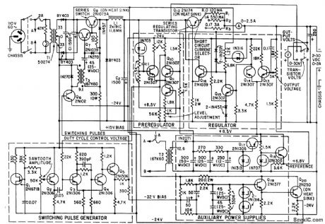
Regulation of short-circuit-proof variable voltage-regulated supply is 0.1 % for 2 to 30 V output and up to 2 amp. Dissipation in series regulating transistor is minimized by controlling on time of series switching transistor Q8. -J. S. Riordon, Power Supply Uses Switching Preregulation, Electronics, 35:10, p 62-64. (View)
View full Circuit Diagram | Comments | Reading(638)
300_mW_25_MHz_AMPLIFIER
Published:2009/7/7 4:25:00 Author:May

Uses quarter-wavelength transmission line T3 in place of parallel-tuned traps to pass even-harmonic currentfreelywh"e blocking odd harmonics Circuit canbe adapted to 300-mW、fvalkie-talkie for 6 or 10meters At 25 MHz、efficiency is 73%,-F, H,Raab,High-Efficiency RF Power Amplifiers,Ham Radio,Oct 1974,p 8-29. (View)
View full Circuit Diagram | Comments | Reading(601)
FAIL_SAFE_TWT_FILAMENT_REGULATOR
Published:2009/7/21 10:33:00 Author:Jessie

Designed to supply well-regulated voltage of 6.3 V d-c at 2 amp to filament of travelling-wave tube, while providing temperature compensation and fail-safe capability. Protective circuit shown in heavy dotted lines operates if one of transistors shorts or if filament voltage rises for any other reason. -G. Stanley, Fail Safe DC Filament Regulator, EEE, 10-6, 32-33. (View)
View full Circuit Diagram | Comments | Reading(1257)
4_BIT_BINARY_TO_5_BIT_BCD
Published:2009/7/7 4:23:00 Author:May
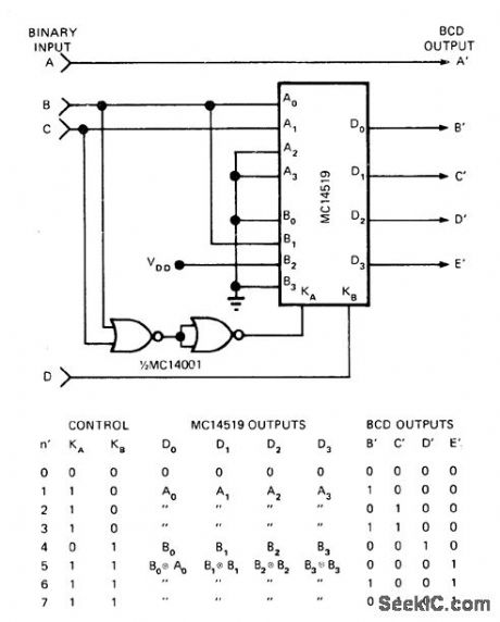
Converts binary number within maohine to BCD value from 0 to 15, for driving visual displays. Requires only quad two-channel data selector with EXCLU-SIVE-NOR function, available in IC packages. Artide gives truth tables and traces operationstep by step.-J. Barnes and J. Tonn, Binaly-to-BCD Converter Implements Simple Algorithm,EDNMagazine, Jan. 5, 1975, p 56, 57, and 59. (View)
View full Circuit Diagram | Comments | Reading(2368)
LOW_FREQUENCY_CONVERTER
Published:2009/7/7 4:23:00 Author:May

Among the signals below 550 kHz are maritime mobile,distress,radio beacons,aircraft weather,European Longwave-AM broadcast, and point-to-point communications. The low-frequency converterconverts the 10to 500 kHz LW range to a 1010 to 1550 kHz MW range,by adding 1000 kHz to all received signals,Radio calibration is unnecessary because signals are received at the AM-radio's dial setting,plus 1MHz;a 100-kHz signal is received at 1100 kHz,a 335-kHz signal at 1335 kHz,etc.The low-frequencysignals are fed to IC1,a doubly-balanced mlxer.
Transistor Q2 and associated circuitry form a Hartley 1000-kHz local oscillator, which is coupled from Q2's drain,through C8,to IC1 pm 8.Signals in the 10-550 kHz range are convened to 1010-1550 kHz.The mixer heterodynes the mcommg low-frequency signal and local-oscillator signal.Transistor Q3reduces IC1's high-output impedance to about 100 Ω to match most recelver inputs.Capacitor C15 couples the 1010-1550 kHz frequencies from Q3's emitter to output jack J3,while blocking any dc bias.
Inductor L6 couples the dc voltage that's carried h the rf signal cable from the rcvr/dc adaptor. The dc voltage and rf signals don't interfere with one another;that saves runmng a separate power-supply wire,which simplifies installation at a remote location.Capacitors C14 and C13 provide dc supply filtering.Thekit is available from North Country Radio,P.O.Box 53,Wykagyl Station,NY 10804.
(View)
View full Circuit Diagram | Comments | Reading(0)
PHASE_REVERSAL_DETECTOR
Published:2009/7/7 4:22:00 Author:May

Used in three-phase applications in which direction of rotation of phases is critical, as in three-phase motors where reversal of two phases can provide disastrous reversal of motor. Line voltages are stepped down and isolated by control-type transformers, Each phase is half-wave rectified and shaped by 1N4001 diode and MPS5172 transistor, with additional shaping by MC14572 inverter. Shaped outputs of all three phases are combined in AND gates G1-G3 to give pulse out-puts sequentially. D flip-flops are connected to sense change in sequence of pulses caused by reversal of one or more input phases. Flip-flop output can be used to trip relay or other protective device for removing air conditioner or other equipment from line before it is damaged.-T. Malarkey, A Simple Line Phase-Reversal Detection Circuit, Motorola, Phoenix, AZ, 1975, EB-54. (View)
View full Circuit Diagram | Comments | Reading(2422)
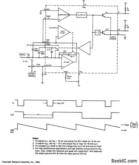
10_Hz_TO_10kHz_V_F_CONVERTER
Published:2009/7/7 4:20:00 Author:May
View full Circuit Diagram | Comments | Reading(545)
TELEFAX_PHASING
Published:2009/7/7 4:17:00 Author:May
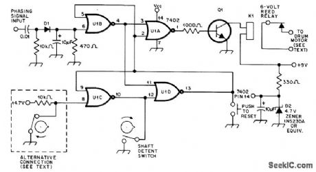
Simple coincidence circuit provides reliable synchronization of Telefax machine in which 2500-Hz signal is generated by photoelectric scanning of paper placed on revolving drum. Circuit uses 7402 quad twoinput NOR gate. If alternate connection enclosed in dashed line is not used, connect pin 8 to ground at pin 7. Q1 is S0014 silicon or equivalent. If relay contacts will handle motor voltage and current, they can be connected directly across points of test switch on machine, with switch left open for phasing circuit to work.-W. C. Smith, A Logic Circuit for Phasing the Telefax, QST, Nov. 1978, p 33-34. (View)
View full Circuit Diagram | Comments | Reading(1333)
TTL_COMPATIBLE_SCHMITT_TRIGGER
Published:2009/7/7 4:15:00 Author:May


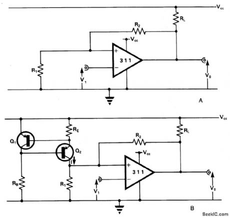
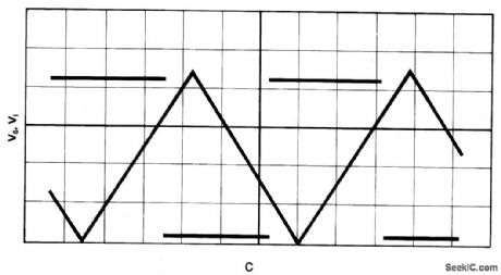
The comparator has an output pull-up resistor RL. and is connected up to operate as a Schmitt trigger using the single rail supply Vcc. The feedback resistors R1 and R2 give upper and lower threshold levels VT+ , VVVTW, respectively. VT+ , is easily set by suitable resistor selection but there is little independent choice of VT- because VT- cannot exceed VCE(SAT) In Fig. 15-13B current-source, comprising the transistors RE, Rg produces a current I~:(VEB/RE), VEB (~0.65 V) being the emitter-base voltage of Q1 and Q2. Fig. 15-13C shows the results of a practical test using the circuit of Fig.15-13B, and the following operating and component data: Vcc=5 V; RL = 1 K ohm; R1=R2=10 K ohm; RB=3.6 K ohm; RE=1K ohm + 10 K ohm pot; Q1=ZTX500; Q2 - ZTX500. (View)
View full Circuit Diagram | Comments | Reading(691)
HIGH_LEVEL_CMOS_CONTROL
Published:2009/7/7 4:14:00 Author:May
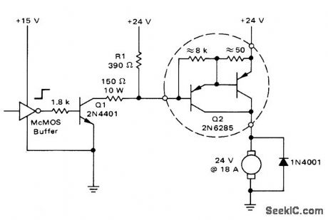
When output of CMOS buffer goes high, Q1 turns on and sinks 150-mA base current of power Darlington Q2, to activate motor load. Used in logic-controlled industrial applications.-A. Pshaenich, Interface Techniques Between Industrial Logic and Power Devices, Motorola, Phoenix, AZ, 1975, AN-712A, p 18. (View)
View full Circuit Diagram | Comments | Reading(643)
MOTOR_STEP_ANGLE_DISPLAY
Published:2009/7/7 4:12:00 Author:May

DigitaI display circuit tracks stepper-motor shaft movements. Up/down decade counters read out four BCD digits as travel angle (000.0 to 360.0) in degrees and number of completed revolutions (0 to 9). Stepper under study is driven by state generator that produces high-current square-wave pulses under control of clock used for display, which can be external square-wave generator or clock output of microprocessor such as KIM-1:. Power source for digital display is 5 V at 1.2 A. Applications include monitoring movements of incremental plotters, precision film camera drives, numerical control machines, and precision start-stop motions of fuel control rods in nuclear reactor.-H. Lo, Digital Display of Stepper Motor Rotation, Computer Design, April1978, p 147-148 and 150-151.
(View)
View full Circuit Diagram | Comments | Reading(2060)
LED_FREQUENCY_COMPARATOR
Published:2009/7/7 4:10:00 Author:May
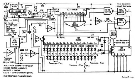
The circuit provides unambiguous LED + or - bar readout with steps of 0.1%. The reference frequency is multiplied by the PLLIC1 and divider IC9 to output 64 x F (ref) and this is then gated by dividing F (measure) by 32 in IC8 thus is F (ref) -(measure) then IC2 counts 1024 pulses. Should the count be more than 1031 than the t latch IC4c/IC4a is set to indicate count too high (F (measure) F (ref)) and if the count is less than 1017 then IC3/IC4b indicate count too low (F(measure) F (ref). These signals are latched by IC5 at the end of each period by the latch signal from IC6e.When the two frequencies are within + or - 0.670 the LSB's of the counter IC2 are decoded and latched by IC7 and displayed on LED's IC6c resets the counter after latching the data. (View)
View full Circuit Diagram | Comments | Reading(1216)
PUT_LONG_DURATION_TIMER
Published:2009/7/7 4:08:00 Author:May
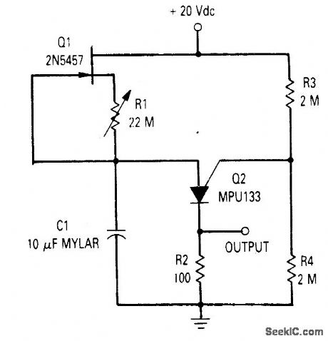
The time circuit can provide a time delay of up to 20 minutes. The circuit is a standard relaxation oscillator with a FET current source in which resistor R1 is used to provide reverse bias on the gate-to-source of the JFET. This tums the JFET off and increases the charging time of C1. C1 should be a low leakage capacitor such as a mylar type.
(View)
View full Circuit Diagram | Comments | Reading(754)
_TIMER_CIRCUIT
Published:2009/7/7 4:08:00 Author:May
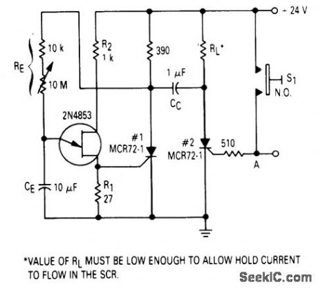
After one cycle of operation, SCR 1 will be on, and a low value of voltage is applied to the UJT emitter circuit, interrupting the timing function. When pushbutton S1 is pushed, or a positive going pulse is applied at point A, SCR 2 will turn on, and SCR 1 will be turned off by commutating capacitor CC. With SCR 1 off, the supply voltage will be applied to RE and the circuit will begin timing again. After a period of time determined by the setting of RE, the UJT witt fire and turn SCR 1 on and commutate SCR 2 off. The time delay is determined by the charge time of the capacitor
(View)
View full Circuit Diagram | Comments | Reading(677)
| Pages:995/2234 At 209819829839849859869879889899909919929939949959969979989991000Under 20 |
Circuit Categories
power supply circuit
Amplifier Circuit
Basic Circuit
LED and Light Circuit
Sensor Circuit
Signal Processing
Electrical Equipment Circuit
Control Circuit
Remote Control Circuit
A/D-D/A Converter Circuit
Audio Circuit
Measuring and Test Circuit
Communication Circuit
Computer-Related Circuit
555 Circuit
Automotive Circuit
Repairing Circuit