
Circuit Diagram
Index 990
VARIABLE_SENSITIVITY_TRIGGER
Published:2009/7/21 9:06:00 Author:Jessie

Biased diode in feedback circuit prevents regeneration.Feedback cannot occur until negative-going pulse greater then bias appears at plate of secondary-emission pentode. Diode bias varies sensitivity, allowing use as pulse-height discriminator also.-E. J. Martin, Jr., How to Use the Secondary-Emission Pentacle, Electronics, 33:41, p 60-63. (View)
View full Circuit Diagram | Comments | Reading(523)
NEGATIVE_PULSE_TRIGGER
Published:2009/7/21 9:05:00 Author:Jessie

Diode is not necessary in input circuit of secondary-emission pentode, since feedback is from dynode to control grid and negative trigger pulse is impressed on cathode. Used in high-speed, short-duration pulse work.-E. J. Martin, Jr., How to Use the Secondary-Emission Pentode, Electronics, 33:41, p 60-63. (View)
View full Circuit Diagram | Comments | Reading(658)
DIODE_COUPLED_SCHMITT
Published:2009/7/21 9:05:00 Author:Jessie

Uses include pulse width modulation of d-c voltage for switching amplifiers, wave shaping, and voltage or current monitoring. Low dynamic resistance of diode formed by Q2 keeps hysteresis (difference between turn-on and turn-off) down to 10 mv.-D. D. Robinson, Diode. Coupled Schmitt Trigger, Electronics, 37:31, p 50-51.
(View)
View full Circuit Diagram | Comments | Reading(652)
REGULATED_DC_DC_CONVERTER
Published:2009/7/7 5:44:00 Author:May
View full Circuit Diagram | Comments | Reading(997)
TOUCHOMATIC
Published:2009/7/7 5:39:00 Author:May
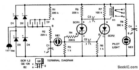
When someone touches the touchplate (TP), the resistance of his finger across points A and B is added in series to the combination of R1 and R2, the capacitor C2 begins to charge. When the voltage across C1 is finally sufficient to fire NE1, C1 will begin to discharge. When NE1 fires, it produces a short between its terminals. Since R3 is connected across C1, they are effectively in series after NE1 fires. A voltage spike will then be passed by C2 and this will act as a positive triggering pulse. The pulse is fed to both SCR gates: SCR2 conducts, there by closing relay K1. With a finger no longer on the touchplate, no more pulses are forthcoming because the C1 charge path is open.The next contact with the touchplate will produce a pulse which triggers SCR1. SCR2 is now off by capacitor C3 which was charged by current passing through R6 and SCR2.The firing of SCR1 in this way places a negative voltage across SCR2 which momentarily drops the relay current to a point below the holding current value of SCR2. (Holding current is the minimum current an SCR requires to remain in a conducting state once its gate voltage is removed.) With SCR2 turned off, the relay will open and SCR1 will turn off due to the large resistance in series with its anode. Starved in this way SCR1 turns off because of a forced lack of holding current. (View)
View full Circuit Diagram | Comments | Reading(748)
TOUCH_SWITCH
Published:2009/7/7 5:38:00 Author:May
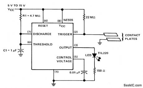
The circuit is basically a NE555 monostable, the only major difference being its method of triggering. The trigger input is biased to a high value by the 22 M ohm resistor. When the contact plates are touched, the skin resistance of the operator will lower the overall impedance from pin 2 to ground. This action will reduce the voltage at the trigger input to below the 1/3 VCC trigger threshold and the timer will start. The output pulse width will be T = 1.1 R1C1, in this circuit about 5 seconds. A relay connected from pin 3 to ground instead of the LED and resistor could be used to perform a switching function. (View)
View full Circuit Diagram | Comments | Reading(0)
PULSE_HEIGHT_TO_WIDTH_CONVERTER
Published:2009/7/7 5:37:00 Author:May

The output-pulse width from the circuit is a linear function of the input pulse's height. You can set the circuit's input threshold to discriminate against low-level pulses, while fixed components limit the circuit's maximum output-pulse width.
With a 270-KΩ resistor connected from the -9 V supply to the base lead of Q2, this circuit can handle input pulses separated by 20 μs for correct operation. The turn-off time of zener diode D2 sets the lower limit for the input-pulse repetition rate.
IC1, D1, and C3 detect the peak of the input pulse. The comparator IC2, triggers at your preset threshold. The RC delay network, R9 and C5, hold off inverter IC3's changing state until the completion of peak detection. After IC3A changes state, Q1 turns on and then turns on Q2, a constant-current source.
Constant-current source Q1 then discharges C3, the peak-detecting capacitor. When C3 has discharged below IC2's threshold, IC2's output decreases, as do pins 6 and 4 of IC3. The output-pulse width is a function of this discharge time, which you can adjust with R6. C6 and R7 control the maximum output-pulse width, which is 8 μs max. (View)
View full Circuit Diagram | Comments | Reading(0)
TOUCH_ON_OFF_SWITCH
Published:2009/7/7 5:36:00 Author:May
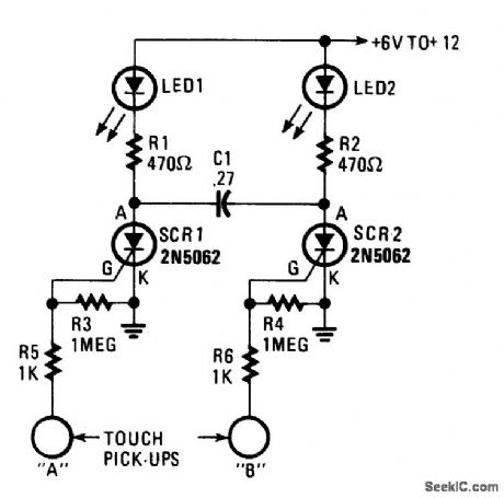
If a Touch On/Off Switch is desired, this circuit fills the bill. Two sensitive gate SCRs are interconnected, so that when one of the devices is turned on, the other (if on) is forced off. That toggling effect gives an on/off circuit condition for each of the LEDs in the SCR-anode circuits. To turn LED1 on and LED2 off, simply touch the A terminal, and to turn LED1 off and LED2 on, the B pick-up must be touched. It is possible to simultaneously touch both terminals, causing both SCRs to turn on together. To reset the circuit to the normal one-on/one-off condition, momentarily interrupt the circuit's dc power source. Additional circuitry can be connected to the anode circuit of either or both SCRs to be controlled by the on/off function of the touch switch. (View)
View full Circuit Diagram | Comments | Reading(1593)
PASSIVE_TONE_CONTROL_CIRCUIT
Published:2009/7/7 5:35:00 Author:May
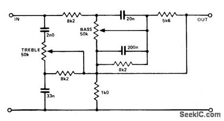
A simple circuit using two potentiometers and easily available standard value components provides tone control. The impedance level is suitable for low-level transistor or op amp circuitry. (View)
View full Circuit Diagram | Comments | Reading(1664)
2_3O_MHz_3OO_W_LlNEAR
Published:2009/7/7 5:34:00 Author:May
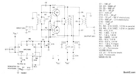
Motorola MRF422 high-power transistors connected in push-pull provide 300 W of PEP or CW output power across band. Uses MPC1000 regulator rated for 10 A and dissipation of 100 W with proper heatsink. Since average base current of transistors is less than 500 mA, however, regulator can be used without heatsink. T1 and T3 have 9:1 impedance ratio, obtained with 1/8-inch copper-braid secondary through which 3 turns of No.22 are wound for primary on Stackpole dual balun ferrite core 57-1845-24B. T2 has 5 turns of two twisted pairs No. 22 enamel wound on Stackpole 57-9322 toroid.-H. Granberg, Get 300 Watts PEP Linear Across 2 to 30 MHz from This Push-Pull Amplifier, Motorola, Phoenix, AZ. 1978, EB-27. (View)
View full Circuit Diagram | Comments | Reading(3365)
LOW_COST_HIGH_LEVEL_PREAMP_AND_TONE_CONTROL_CIRCUIT
Published:2009/7/7 5:34:00 Author:May

This preamp and tone control uses the JFET to its best advantage; as a low noise high input impedance device. All device parameters are noncritical, yet the circuit achieves harmonic distortion levels of less than 0.05% with a S/N ratio of over 85 dB. The tone controls allow 18 dB of cut and boost; the amplifier has a 1-V output for 100-mV input at maximum level. (View)
View full Circuit Diagram | Comments | Reading(1754)
ZERO_IB_ERROR_V_I_CONVERTER
Published:2009/7/7 5:34:00 Author:May

Single programming resistor RP provides an output-current range of about six decades. Note that this resistor's TC is also a potential source of error; it dissipates 125 mW when VIN= 5 V. The maximum deviation is typically 50 nA or 0.0002% of full scale. This voltage-controlled current source uses optocou-pler IC2 to eliminate an error found in more conventional circuits and which is caused by the output transistor's base current. (View)
View full Circuit Diagram | Comments | Reading(826)
MIKE_PREAMP_WITH_TONE_CONTROL
Published:2009/7/7 5:33:00 Author:May
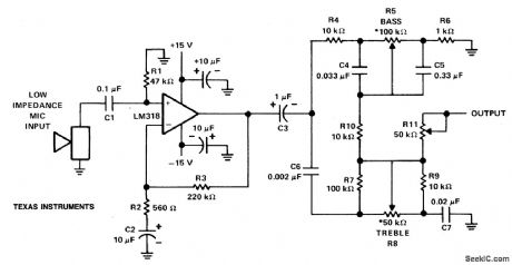
The LM318 op amp is operated as a standard noninverting amplifier. Resistor R1 (47 k ohm) provides an input path to ground for the bias current of the non-inverting input. The combination of R2 (560 ohm) and C2 (10 μF) provides a frequency roll-off below 30 Hz. At 30 Hz and above the gain is relatively flat at about 50 dB, set by the ratio R3/R2. R3 (200 k ohm) furnishes negative feedback from the output to the inverting input of the op amp. C3 (1.0 μF electrolytic) ac couples the preamp to the tone control section. The top half of the tone control section is the bass control. The bottom half controls the treble frequency response. These tone controls (R5 and R8) require audio taper (logarithmic) potentiometers. The 50 k ohm potentiometer on the output can be used to set the output or gain of the preamp. (View)
View full Circuit Diagram | Comments | Reading(2606)
PIN_PHOTODIODE_TO_FREQUENCY_CONVERTER
Published:2009/7/7 5:32:00 Author:May
View full Circuit Diagram | Comments | Reading(800)
_TONE_CONTROL_AUDIO_AMPLIFIER
Published:2009/7/7 5:32:00 Author:May


The circuit makes excellent use of the high slew rate, wide bandwidth, high input impedance, and high-output voltage capability of the CA3140 BiMOS op amp. The wideband gain of this circuit is equal to the ultimate boost or cut plus one, in this case a gain of eleven. For 20-dB boost or cut, input loading is essentially equal to the resistance from terminal 3 to ground.
(View)
View full Circuit Diagram | Comments | Reading(688)
AMPLIFIED_ZENER
Published:2009/7/7 5:31:00 Author:May
Combination of 1-W zener and 50-90 W audio trnsistor replaces 50-W zener in developing bias ror high-power tubetype linear amplifier Voltage of zener should be about 0.3 V less than desired bias voltage if using germanium transistor and about 0.7 V less for silicon transistor. Connec-tions are shown for PNP and PNP transistors.Use chassis as heatsink for transistor, with mica insulating washer for NPN. Ferrite beads dis-courage parasitic oscillations.-An Altemative to High-Wattage Zener Diodes, QST, June 1975, p45. (View)
View full Circuit Diagram | Comments | Reading(777)
DATA___MULTIPLEXER_DECODER
Published:2009/7/7 5:30:00 Author:May

CD4013A flip-flop switches channel opamps alternately to transmission line under control of -5 V clock pulses for multiplexing of inputs to line, Any number of input channels can be added by ex tending circuit. At receiving end, one CA3080A variable opamp is used as mono MVBR to provide 10μs delay for input signal to settle before being sampled by sample-and-hold decoder. Either output of flip-flop can be used to trigger MVBR,- Circuit Ideas for RCA Linear ICs, RCA Solid State Division, Somerville, NJ, 1977, p 15. (View)
View full Circuit Diagram | Comments | Reading(1025)
SQUARE_TO_SINE_WAVE_CONVERTER
Published:2009/7/7 5:29:00 Author:May

Two pairs of MOSFETs form a bridge that alternately switches current in opposite directions. Two parallel-resonant LC circuits complete the converter. The L1/C1 combination is resonant at the fundamental frequency; the L2/C2 combination is resonant at the clock frequency's third harmonic and acts as a trap. T1 and C3 ensure that both halves of the MOSFET bridge are never on at the same time by providing a common delay to the gate drive of each half. Select the values of R1 and C3 to yield a time constant that's less than 5% of the clock's period. You can add an output amplifter for additional buffering and conditioning of the circuit's sine-wave output. (View)
View full Circuit Diagram | Comments | Reading(2124)
10W_ON_2_METERS
Published:2009/7/7 5:29:00 Author:May

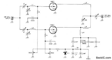
Linear power amplifierfor 2-meter transverter delivers 10 W PEP using two Siliconix VMP1 Mospower FETs. L1 and L2 are 8 turns, and L3 and L4 are 5 turns, all close-wound with No. 20 enamelon 3-mm form. Tran-sistor requires heatsink, insulated from chassis with 0.062-in beryllium oxide insulators. Effi-ciency is about 40%. -L. Leighton, Two-Meter Transverter Using Power FETs, Ham Radio, Sept. 1976, p 10-15. (View)
View full Circuit Diagram | Comments | Reading(665)
432_450_MHz
Published:2009/7/7 5:27:00 Author:May
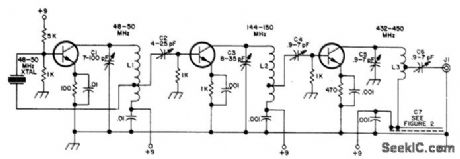
Crystal oscillator stage operating at 48-50 MHz puts out enough power to drive pair of triplers. All transistors are HEP-75.L1 is 20 turns No. 24 on 5-mm form, tapped 8 turns from cold end. L2 is 5 turns No. 20 airwound to 8-mm diameter. L3 is 3 turns No, 20 air-wound to 5-mm diameter, with center tap. rticle covers construction, adjustment, and uses,-B. Hoisington, Getting Started on 450 MHz, 73 Magazine, Nov. 1973, p 21-24. (View)
View full Circuit Diagram | Comments | Reading(636)
| Pages:990/2234 At 209819829839849859869879889899909919929939949959969979989991000Under 20 |
Circuit Categories
power supply circuit
Amplifier Circuit
Basic Circuit
LED and Light Circuit
Sensor Circuit
Signal Processing
Electrical Equipment Circuit
Control Circuit
Remote Control Circuit
A/D-D/A Converter Circuit
Audio Circuit
Measuring and Test Circuit
Communication Circuit
Computer-Related Circuit
555 Circuit
Automotive Circuit
Repairing Circuit

