
Circuit Diagram
Index 992
GUITAR_TREBLE_BOOST
Published:2009/7/7 5:02:00 Author:May
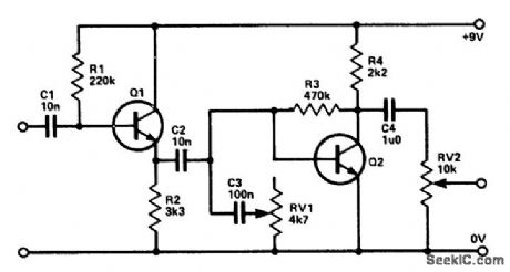
Q1 is connected as an emitter follower in order to present a high input impedance to the euitar. C2, being a relatively low capacitance, cuts out most of the bass, and C3 with RV1 acts as a simple tone control to cut the treble, and hence the amount of treble boost can be altered.Q2 is a simple preamp to recover signal losses in C2, C3, and RV1. (View)
View full Circuit Diagram | Comments | Reading(712)
VOLTAGE_TUNED_CLAPP_OSCILLATOR
Published:2009/7/22 3:44:00 Author:Jessie

This voltage-tuned Clapp oscillator uses a varactor diode to set its operating frequency. D1 is an NTE614. L1 is about 7/ƒ (MHz) microhenries. With the circuit shown, the frequency range is about 6 to 15 MHz. (View)
View full Circuit Diagram | Comments | Reading(785)
Voltage_regulator_for_a_projection_lamp
Published:2009/7/22 3:43:00 Author:Jessie
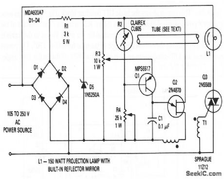
This circuit shows the basic UJT building block (Fig. 9-1), which is used to regulate the voltage across a projection lamp to 100 V (±2%) for an input voltage between 105 and 250 V. This is done by indirectly sensing the light output of lamp L1 and applying the feedback signal to the firing circuit (Q1 and Q2), which controls the conduction angle of triac Q3. The reflector inside the lamp envelope glows red because of the filament heat. Because the reflector has a relatively large mass, the reflector cannot respond to the supply frequency, and the light output provides a form of integration. Photocell R2 is mounted at one end of a black tube, and the other end of the tube is directed at the reflector's back side. R3 and R4 set the lamp voltage to 100 Y when the line voltage is 105 and 250 V, respectively. This assures that the lamp voltage will be within the desired tolerance over the operating range of the input voltage. Some interaction occurs between R3 and R4, and the adjustment of each pot might have to be made several times. Because this is an rms voltage regulator, a true rms meter must be used to adjust the load voltages. (View)
View full Circuit Diagram | Comments | Reading(0)
ADJUSTABLE_AC_TIMER.2_TO_10_SEC
Published:2009/7/7 5:01:00 Author:May

View full Circuit Diagram | Comments | Reading(598)
_PRECISION_ELAPSED_TIME_COUNTDOWN_TIMER
Published:2009/7/7 4:59:00 Author:May
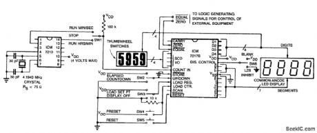
The circuit uses an ICM7213 precision one minute/one second timebase generator using a 4.1943 MHz crystal for generating pulses counted by an ICM7217B. The thumbwheel switches allow a starting time to be entered into the counter for a preset-countdown type timer, and allow the register to be set for compare functions. For instance, to make a 24-hour clock with BCD output the register can be preset with 2400 and the EQUAL output used to reset the counter. Note the 10 k resistor connected between the LOAD COUNTER terminal and ground. This resistor pulls the LOAD COUNTER input low when not loading, there by inhibiting the BCD output drivers. This resistor should be eliminated and SW4 replaced with an SPDT center-off switch if the BCD outputs are to be used. (View)
View full Circuit Diagram | Comments | Reading(2891)
Ultrasonic_receiver
Published:2009/7/22 3:43:00 Author:Jessie

This low-power ultrasonic receiver, built around two MAX403s, can operate for several weeks on a 9-V battery. The receiver has high gain at ultrasonic frequencies to detect faint reflections from a separate ultrasonic source (not shown). To prevent false triggering, the 40-kHz received signal passes through R7 to charge C3 after being rectified by D1. The rectified signal is detected by a MAX406 op amp, connected as a comparator, chosen because of its 1-μA supply current and rail-to-rail output swing. (View)
View full Circuit Diagram | Comments | Reading(6)
BALANCED_MODULATOR_DEMODULATOR
Published:2009/7/22 1:14:00 Author:Jessie

Achieves high carrier and modulation suppression by using closely matched diodes and providing R1 for amplitude adjustment and coaxial line for phase adjustment. R2 provides slight amplitude adjustment.-W. H.Ellis, Diode Quad Modulator Suppresses Carrier 65 Db, Electronics, 39:8, p 97. (View)
View full Circuit Diagram | Comments | Reading(894)
EIGHT_CHANNEL_SEQUENTIAL
Published:2009/7/7 4:59:00 Author:May

Eight different analog inputs are sampled by National LF13508 multiplexor and converted into digital words for furtner processing. Maximum throughput rate of system is 2800 samples per second per channel. Output will settle to ±0.05mV in 1μs after hold command.- FET Data-book, National Semiconductor, Santa Clara, CA, 1977, p 5-77-5-78. (View)
View full Circuit Diagram | Comments | Reading(605)
VOLTAGE_TO__FREQUENCY_USING_IC_TIM_ERS
Published:2009/7/7 4:59:00 Author:May
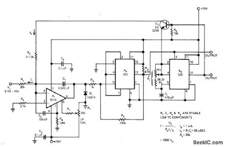
Two 322 IC timers and single 301A opamp provide all functions required for charge-balancing type of voltage-to-frequency converter, including integrator, level sensor or comparator, precision mono, and gated current source. Circuit accepts control voltage inputs of 0 to -10 V, corresponding to output pulse stream range of 0 to 10 kHz. Article describes operation in detail. R4, should be 4.7 megohms. Output pulses of comparator A3 trigger mono A2, which generates pulse having duration t1 that saturates Q1, to force reference current l2, into summing point of opamp integrator.-W.G. Jung, Take a Fresh Look at New IC Timer Applications, EDN Magazine, March 20, 1977, p 127-135. (View)
View full Circuit Diagram | Comments | Reading(1281)
SIREN_WITH_MUTING
Published:2009/7/22 1:13:00 Author:Jessie

National LM389 array having three transistors and power opamp on same chip uses opamp as square-wave oscillator whose frequency is adjusted with R2B. One transistor is used in muting circuit to gate power amplifier on and off, while other two transistors form cross-coupled MVBR that controls rate of square-wave oscillator.- Audio Handbook, National Semiconductor, Santa Clara, CA, 1977, p 4-33-4-37. (View)
View full Circuit Diagram | Comments | Reading(820)
LOW_POWER_MICROPROCESSOR_PROGRAMMABLE_INTERVAL_TIMER
Published:2009/7/7 4:58:00 Author:May

The microprocessor sends out an 8-bit binary code on its 8-bit I/O bus (the binary value needed to program the ICM7240), followed by four WRITE pulses into the CD4017B decade counter. The first pulse resets the 8-bit latch, the second strobes the binary value into the 8-bit latch, the third triggers the ICM7240 to begin its timing cycle and the fourth resets the decade counter. The ICM7240 then counts the interval of time determined by the R-C value on pin 13, and the programmed binary count on pins 1 through 8. At the end of the programmed time interval, the interrupt one-shot is triggered, informing the microprocessor that the programmed time interval is over. With a resistor of approximately 10 M ohm and a can capacitor of 0.1,ttF, the time base of the ICM7240 is one second. Thus, a time of 1-255 seconds can be programmed by the microprocessor, and by varying R or C, longer or shorter time bases can be selected. (View)
View full Circuit Diagram | Comments | Reading(1173)
Basic_triac_switches
Published:2009/7/21 22:03:00 Author:Jessie
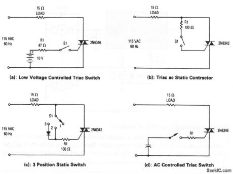
These circuits show triacs that are used to control a pure resistive load (of about 7 A) across an ac line. In Fig. 8-5A, gate current is supplied to the triac from the 10-V battery when S1 is closed. The triac tums on and remains on until S1 is opened. This cirquit switches at zero current, except for initial turn on, so S1 can be a very low-current switch (carring only triac gate current). The triac switch of Fig.8-5B has the same characteristics as Fig. 8-5A, except that the battery is eliminated. In the circuit of Fig. 8-5C, when S1 is in position 1, the triac receives no gate current and is nonconducting. With S1 in position 2, operation is the same as in Fig. 8-5B. With S1 in position 3, the triac receives gate current only on positive half-cycles, and power to the load is half-wave. Figure 8-5D shows ac control of the triac. (View)
View full Circuit Diagram | Comments | Reading(1491)
BCD_FROM_7_SEGMENT_DISPLAY
Published:2009/7/7 4:56:00 Author:May

Single National DM76L25 read-only memory provides conversion from 7-segment outputs of MOS chip driving display to BCD inputs for data processing. Typical power dissipation is 75 mW. Access time is 70 ns when using 5-V supply. Article gives truth table for all standard and special characters of 7-segment display.-U. Priel, 7-Segment-to-BCD Converter: The Last Word?, EDN Magazine, Aug. 20, 1974, p 94-95. (View)
View full Circuit Diagram | Comments | Reading(2038)
SPLIT_PHASE_CONTROL_WITH_BRAKING
Published:2009/7/7 4:55:00 Author:May
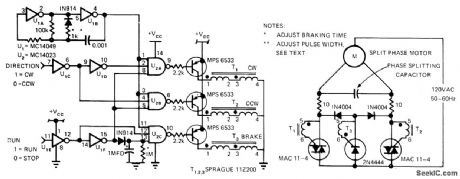
Use of CMOS logic to gate direction-controlling triacs and turn on SCR for braking provides lowcost switchless control of split-phase motor used In place of brush-type DC motor Aρplications include control of ball valves and other throtting functions in process control With shaft-position encoders, circuit generates feed-back information. Overshoot and other stability problems are easily controlled by strong braking function. CMOS logic provides complete noise immunity. Oscillator pulse width is adjusted with 1K resistor in series with 1N914, and brake duration is controlled by 1-megohm resistor at input of U2C. With values shown, brake is applied for about 1 s. Circuit works reliably on supply voltages of 5 to 15 V.-V. C. Gregory, Split-Phase Motor Control Accomplished with CMOS, EDN Magazine, 0ct. 5, 1974 p 65-67. (View)
View full Circuit Diagram | Comments | Reading(1396)
CROWBAR_IGNITRON
Published:2009/7/21 22:03:00 Author:Jessie

Multimegawatt high-vacuum modulator tubes for large radars are protected during tests by circuit that is triggered by fault sensors. Total response time for firing ignitron crowbar is below 10 microsec.-T. E. Yingst, Circuits to Control and Protect High-Power Modulator Tubes, Eleatronics, 35:4, p 56-61. (View)
View full Circuit Diagram | Comments | Reading(950)
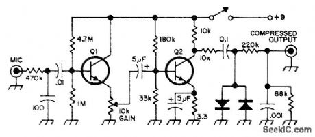
PRECOMPRESSION_SHAPER
Published:2009/7/21 22:03:00 Author:Jessie

Improves effective signal strength of SSB transmitter by shaping AF frequency response ahead of audio compressor. Low-noise FET preamp providing initial gain for high-impedance microphone is followed by low- and high-rolloff circuit giving 15-dB boost or roll off to frequencies centered at about 1 kHz.-J. J. Schultz, Adding dBs to the Audio Compressor, 73 Magazine, May 1974, p 21-23 and 25. (View)
View full Circuit Diagram | Comments | Reading(1363)
PREAMP_WITH_CLIPPING
Published:2009/7/21 22:01:00 Author:Jessie
Increases speech intelligibility, particularly with SSB amateur stations Q1 and Q2 are HEP-54 Diodes are 1N456 or HEP-158.-Circuits,73 Magazine, Feb,1974.p100. (View)
View full Circuit Diagram | Comments | Reading(612)
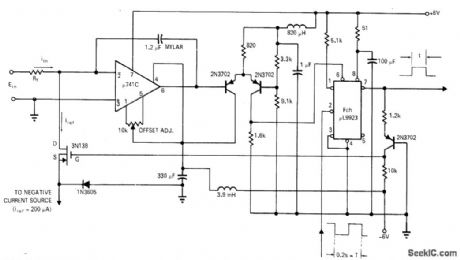
CHARGE_DISPENSING_V_F_CONVERSION
Published:2009/7/7 4:55:00 Author:May

Output state of opamp switches C1 between reference voltage provided by diode bridge and its inverting input. Network R2-C2 reinforces direction of opamp output change. Circuit can deliver 0-10 kHz output with 0.01% linearity for 0-10 V input. -J. Williams, Low-Cost, Linear A/D Conversion Uses Single-Slope Techniques, EDN Magazine, Aug, 5, 1978, p 101-104. (View)
View full Circuit Diagram | Comments | Reading(870)
ANALOG_TO_PULSE_WIDTH
Published:2009/7/7 4:53:00 Author:May
Stripped-down version of dual-slope A/D converter integrates input current constantly but switches reference current into integrator each time clock pulse occurs. Accuracy of 0.1% makes circuit suitable for use in digital voltmeter. Reference current is switched out of integrator when output voltage reaches +4.5V. With values shown, using 100 kilohms for R1, maximum input current is 80 μA and full-scale voltage is 8 V. Article includes timing diagram and design equations.-N. A. Robin, Analog-to-Pulse-Width Converter Yields 0.1% Accuracy, EDN Magazine, Nov. 1, 1970, p 42-43. (View)
View full Circuit Diagram | Comments | Reading(960)
Read_circuitry_of_paper_tape_reader_for_RTL
Published:2009/7/21 21:26:00 Author:Jessie

Read circuitry of paper-tape reader for RTL (courtesy Motorola Semiconductor Products Inc.). (View)
View full Circuit Diagram | Comments | Reading(698)
| Pages:992/2234 At 209819829839849859869879889899909919929939949959969979989991000Under 20 |
Circuit Categories
power supply circuit
Amplifier Circuit
Basic Circuit
LED and Light Circuit
Sensor Circuit
Signal Processing
Electrical Equipment Circuit
Control Circuit
Remote Control Circuit
A/D-D/A Converter Circuit
Audio Circuit
Measuring and Test Circuit
Communication Circuit
Computer-Related Circuit
555 Circuit
Automotive Circuit
Repairing Circuit