
Circuit Diagram
Index 989
SUPPLY_OVERLOAD_AND_REVERSE_POLARITY_PROTECTION
Published:2009/7/21 10:03:00 Author:Jessie
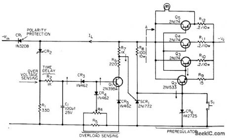
Uses signal from Q1 to trigger SCR1, which turns off series-pass transistor when overload reaches 15 amp. Will also provide limiting of output voltage at 25 V, input overvoltage protection at 32 V, and input reverse-polarity protection by CRL. -J. J. Rado, Versatile SCR Protection for Power Supplies, EEE, 13:8, p 56-62. (View)
View full Circuit Diagram | Comments | Reading(1059)
FOUR_STAGE_PNPN_BINARY_COUNTER
Published:2009/7/21 9:21:00 Author:Jessie

Operates on negative trigger pulses, to provide 16:1 division.-J. B. Hangsfefer and L. H. Dixon, Jr., Triggered Bistable Semiconductor Circuits, Electronics, 32:35, p 58-60. (View)
View full Circuit Diagram | Comments | Reading(625)
ADJUSTABLE_SCHMITT_TRIGGER
Published:2009/7/21 9:21:00 Author:Jessie
Accepts either sine waves or pulses. Adjustable input level control allows trigger to occur on any desired portion of input waveform. Amplifier stage drives flip-flop of units decade counter directly.-R. W. Wolfe, Decode Decimal Counter Speeds Printed Readout, Electronics, 31;3, p 88-90. (View)
View full Circuit Diagram | Comments | Reading(882)
BLOCKING_OSCILLATOR_TRIGGER_GENERATOR
Published:2009/7/21 9:20:00 Author:Jessie

Generates relatively narrow pulses at adjustable repetition rate. Audio transformer provides positive feedback.-H. L. Armstrong, Transistorized Trigger and Delay Generators, Electronics, 313, p 96-98. (View)
View full Circuit Diagram | Comments | Reading(578)
COMBINATION_SCHMITT_MONOSTABLE
Published:2009/7/21 9:20:00 Author:Jessie

Three transistors in complementary connection give Schmitt trigger (Q1-Q2) und mono-stable mvbr (Q2-Q3) in which triggering level is accurately controlled. Output pulse width is independent of input because circuit is regenerative.-G. Marosi, Combination Schmitt Trigger-Monostable Multivibrator, EEE, 13:10, p 77. (View)
View full Circuit Diagram | Comments | Reading(681)
COLLECTOR_TRIGGERING_WITH_TRIG0ER_AM_PLIFIER
Published:2009/7/21 9:19:00 Author:Jessie

Used in early stages of counter to increase speed, while permitting automatic assembly in all stages. For 1-Mc trigger rate, less than 1 v of positive trigger amplitude is needed.- Transistor Manual, Seventh Edition, General Electric Co., 1964, p 198. (View)
View full Circuit Diagram | Comments | Reading(515)
RANDOM_PULSE_DETECTOR
Published:2009/7/21 9:18:00 Author:Jessie

Either positive or negative pulses above predetermined minimum amplitude force Q1 into saturation and turn Q2 off, causing the meter to deflect immediately. Circuit may also be used as pulse stretcher or threshold detector.-C. F. Johnson and J. T. Loiselle, Bipolar Pulse Detector Features Meter Display, Electronics, 38:24, p 63. (View)
View full Circuit Diagram | Comments | Reading(572)
PULSE_GENERATOR
Published:2009/7/21 9:17:00 Author:Jessie

Delivers 1-amp peak out put current having duration of 10 microsec when pnpn unit is triggered on by low-level positive pulse applied to its base.-J. B. Hangstefer and L. H. Dixon, Jr., Triggered Bistable Semiconductor Circuits, Electronics, 32:35, p 58-60. (View)
View full Circuit Diagram | Comments | Reading(0)
HOURS_OF_DELAY
Published:2009/7/21 9:16:00 Author:Jessie

Capacitor starts charging from -12 v to +12 v when switch is opened.Diode begins conducting at ground potential, and operational trigger trips when diode passes 2 na. Timing accuracy is high.-P. Lefferts, Operational Trigger For Precise Control, Electronics, 37:28, p 50-55. (View)
View full Circuit Diagram | Comments | Reading(693)
SATURATED_TRANSISTOR_MEASUREMENT
Published:2009/7/21 9:16:00 Author:Jessie

Transistor under lest is biased to saturate collector to within 100 my of ground for 10-ma collector load. Operational trigger then trips when Vx is 1 mv above 100 my.-P. Lefferts, Operational Trigger For Precise Control,Electronics,37:28,p 50-55. (View)
View full Circuit Diagram | Comments | Reading(622)
VARIABLE_HYSTERESIS_SCHMITT
Published:2009/7/21 9:15:00 Author:Jessie

R7 adjusts lower trigger point, and R8 adjusts upper trigger point.-R. S. Hughes, Variable-Hysteresis Schmitt Trigger, EEE, 13:7, p 41. (View)
View full Circuit Diagram | Comments | Reading(734)
BASE_TRIGGERED_FLIP_FLOP
Published:2009/7/21 9:14:00 Author:Jessie

Maximum trigger rate for steering circuit exceeds 5 Mc with negative trigger pulse amplitude from 0.75 to 2 v. Requires less trigger energy than collector triggering but more accurately controlled trigger amplitude.- Transistor Manual, Seventh Edition, General Electric Co., 1964, p 197. (View)
View full Circuit Diagram | Comments | Reading(555)
SENSE_AMPLIFIER
Published:2009/7/21 9:13:00 Author:Jessie

Blocking-oscillator transistor amplifier is triggered by output of diode bridge network. Rectification assures that readout voltages of both polarities are sensed.Diodes attenuate small signals greatly relative to large signals, increasing signal-noise ratio at rectifier output to about 20:1.-C. S. Warren, W. G. Rumble, and W. A. Helbig, Transistorized Memory Monitors Earth Satellite, Electronics, 31:3, p 66-70.
(View)
View full Circuit Diagram | Comments | Reading(1)
LC_PULSE_GENERATOR
Published:2009/7/21 9:12:00 Author:Jessie

Provides half-sinusoid output determined by L and C, when pnpn unit is triggered on by low-level positive pulse applied to its base.-J. B. Hangstefet and L. H. Dixon, Jr., Triggered Bistable Semiconductor Circuits, Electronics, 32:35, p 58-60. (View)
View full Circuit Diagram | Comments | Reading(758)
HIGH_IMPEDANCE_SCHMITT
Published:2009/7/21 9:12:00 Author:Jessie

Use of let Q1 for input stage gives high input impedance, as required for threshold detector circuit. Output pulse is square wave at up to 100 kc triggering. Turnoff threshold is about 0.2 v below turnon.-L. R. Lott, FET Increases Schmitt Trigger Input Impedance, Electronics, 38:15, p 65. (View)
View full Circuit Diagram | Comments | Reading(1202)
REGENERATIVE_SWITCHING_TRIGGER
Published:2009/7/21 9:11:00 Author:Jessie

Advantages over conventional Schmitt include reduced power consumption (neither transistor conducts during off state), full range output voltage swing, and low output Impedance. Some input signal appears in output. Rise and fall times are 0.15 microsec.-R. K. Vieth, Trigger Circuit Gives Less P-diss, More V-out, EEE, 11:12,p 28. (View)
View full Circuit Diagram | Comments | Reading(868)
VOLTAGE_MONITOR
Published:2009/7/21 9:09:00 Author:Jessie

Input voltage sensitivity better than 0.7 mv is obtained from operational trigger.-P. Lelferts, Operational Trigger For Precise Control, Electronics, 37:28, p 50-55. (View)
View full Circuit Diagram | Comments | Reading(1)
DELAYED_TRIGGER_GENERATOR
Published:2009/7/21 9:08:00 Author:Jessie

Provides controllable positive or negative delayed trigger. When used to see leading edge of multivibrator pulse on cro, trigger starts cro sweep and delay generator. After preset time, delay generator produces pulse used to trigger mvbn-H. L. Armstrong, Transistorized Trigger and Delay Generators, Electronics, 31:3, p 96-98. (View)
View full Circuit Diagram | Comments | Reading(806)
NONCUTOFF_SCHMITT
Published:2009/7/21 9:07:00 Author:Jessie
Both amplifiers are always connected to their current sources, hence are never cut off and can operate in optimum region, with no risk of damage by inverse base-emitter voltage. Output voltage alternates between two levels.-H. Inose, Y, Yoshida, and H. Tada, Noncutoff Circuits Improve Trigger Switching, Electronics, 35:30, p 36-39. (View)
View full Circuit Diagram | Comments | Reading(567)
PNPN_FLIP_FLOP_BINARY_COUNTER
Published:2009/7/21 9:06:00 Author:Jessie

Negative trigger pulses produce 2:1 operation. Con be driven from identical flip-flop or from collector of npn silicon transistor.-J. B. Hang-stefer and L. H. Dixon, Jr., Triggered Bistable Semiconductor Circuits, Electronics, 32:35, p 58-60. (View)
View full Circuit Diagram | Comments | Reading(555)
| Pages:989/2234 At 209819829839849859869879889899909919929939949959969979989991000Under 20 |
Circuit Categories
power supply circuit
Amplifier Circuit
Basic Circuit
LED and Light Circuit
Sensor Circuit
Signal Processing
Electrical Equipment Circuit
Control Circuit
Remote Control Circuit
A/D-D/A Converter Circuit
Audio Circuit
Measuring and Test Circuit
Communication Circuit
Computer-Related Circuit
555 Circuit
Automotive Circuit
Repairing Circuit