
Circuit Diagram
Index 390
The circuit of Buick GL8 automobile ABS, bonding, ABS electronic control unit and traction electronic control unit EBCMEBTCM
Published:2011/8/30 1:47:00 Author:Jessie | Keyword: Buick , automobile ABS, bonding, electronic control unit , traction , electronic control unit, EBCMEBTCM

View full Circuit Diagram | Comments | Reading(745)
The circuit of IC decoder on the EPSON ink cartridge
Published:2011/8/30 1:45:00 Author:Jessie | Keyword: IC decoder, EPSON ink cartridge

View full Circuit Diagram | Comments | Reading(3311)
Glanze WD-900B microwave oven principle circuit
Published:2011/8/30 1:44:00 Author:Jessie | Keyword: microwave oven, Glanze
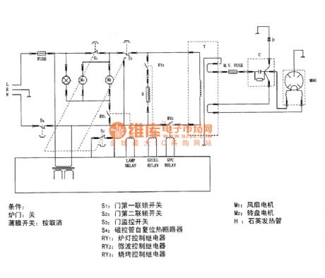
R1-The first door interlock switch; S2-the second door interlock switch; S3-door monitoring switch, S4-magnetron self-resetting thermal breaker, RY1-oven light control relay, RY2-microwave control relay, RY3 - BBQ control relay, M1-fan motor, M2-wheel motor, H-quartz heating tube. (View)
View full Circuit Diagram | Comments | Reading(2368)
Rongsheng heat insulation automatic electric cooker principle diagram
Published:2011/8/30 1:40:00 Author:Jessie | Keyword: Rongsheng , heat insulation, automatic electric cooker

View full Circuit Diagram | Comments | Reading(747)
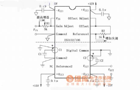
The gain adjustment, detuning regulation and bandwidth control circuit of ISO102/106
Published:2011/8/30 1:39:00 Author:Jessie | Keyword: gain adjustment, detuning regulation , bandwidth control
View full Circuit Diagram | Comments | Reading(648)
830MHz medium power amplifier principle circuit composed of RF2104
Published:2011/10/26 21:36:00 Author:May | Keyword: medium power amplifier principle

Radio-frequency signal (RF) is input by pin 5, output by pin 12 after being amplified by the pre-amplifier, last stage power amplifier. pin 5 has the DC voltage, therefore it is added the separating direct coupling capacitor and simultaneously connected to divergence inductance (10nH) in parallel, pin 5's input impedance is 50Ω. The output end's pin 12, 13 are connected, usually, pin 13, 14 are connected outside to be used as the signal output, and the output connects the matching network to make the amplifier output impedance match with it, when the pin's loaded impedance is 5+10Ω, itmay obtain the peak power output. pin 13, 14 are connected outside to be used as the last stage power amplifier's power source end. (View)
View full Circuit Diagram | Comments | Reading(689)
Low-power consumption AC flashing light circuit diagram
Published:2011/10/26 21:49:00 Author:May | Keyword: Low-power consumption , AC flashing light
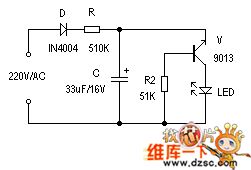
It uses the charging and discharging characteristic of capacitor C and the negative resistance characteristic of triode V under the breakdown condition to constitute a squegger oscillator. After getting power, 220V alternating current is half-wave rectified by diode D, current limited by resistor R to charge for C. When C's both sides voltage rises to V's breakdown voltage ( the actual value is approximately 9V), then it rapidly discharges by V to make the LED connected in discharging loop illuminate. After the discharging ended, V regains the closure condition, C starts to charge and to be redundant the above process. V has the synchronized signal which added to base to trigger the avalanche. Electric circuit working actual value is only 0.17mA. (View)
View full Circuit Diagram | Comments | Reading(1655)
High input-high output integrated regulated power supply circuit circuit diagram 2
Published:2011/8/19 2:30:00 Author:Jessie | Keyword: High input-high output , integrated regulated power supply

View full Circuit Diagram | Comments | Reading(688)
High input-high output integrated regulated power supply circuit circuit diagram 1
Published:2011/8/19 2:30:00 Author:Jessie | Keyword: High input-high output , integrated regulated power supply

View full Circuit Diagram | Comments | Reading(718)
Auto voltage monitoring circuit diagram
Published:2011/8/19 2:34:00 Author:Jessie | Keyword: Auto voltage monitoring
This circuit is applied to supervise if auto power supply voltage12V is normal or not. If the power supply voltageis 12~14.5 V, then it is normal, whenit is lower than 12V or higher than 14.5V,the indicator will be lit up. A(1), A(2) are indicator comparators for adjusting potentiometers W (1), W (2). When thecar's power supply voltage is higherthan 1.45 V, lamp B is on; or it is lower than 12V,lamp A is on;Normal, these two lights are not bright. (View)
View full Circuit Diagram | Comments | Reading(730)
50HZ time-base signal generator circuit diagram
Published:2011/10/26 21:57:00 Author:May | Keyword: 50HZ , time-base signal generator
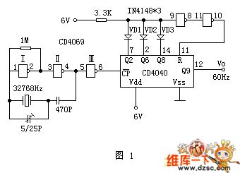
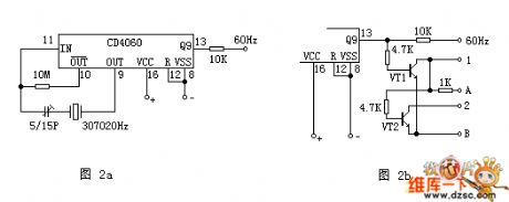
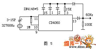
The attached figure 1 is the 60Hz digit-clock time-base circuit composed of the 12-bit binary serial counter/frequency divider CD4040 and six phase reverser CD4069 and so on. In the circuit, the CD4069's gate I and gate II constitute the crystal oscillator with oscillating frequency in 32768Hz. Chart 2a is another kind of 60Hz pulse generating circuit. It consists of the integrated circuit CD4060 and crystal oscillator with the resonance frequency in 30720Hz. CD4060 is 14-bit binary serial counter, frequency divider and oscillator. The CD4060's interior divides into two parts, one part is 14-level counter/frequency divider, and its frequency division coefficient is 16¯16348.
(View)
View full Circuit Diagram | Comments | Reading(8532)
RF2126 high power linear amplifier pin circuit diagram
Published:2011/10/26 22:00:00 Author:May | Keyword: high power linear amplifier

RF2126 is high-power, high-efficiency linear amplifier IC. It adopts advanced GaAs hetero-junction bipolar transistor (HBT) technology. It is designed for 2.5GHz ISM frequency range final linear RF amplifier, such as WLAN and POS terminal, it also can beused for digital PCS phone to send out final linear enlarging. Its working frequency is 1800~2500MHz.RF2126 has matching network, and RF2126 itself includes power supply wire and bypass capacitor. Output power’s typical value is 1W. RF2126 can beused for 2.5Hz ISM frequency range, digital communication system, PCS communications system, commercial and consumer system, portable battery power equipment and so on. RF2126’s pin array and functionare shown in the following diagram.
(View)
View full Circuit Diagram | Comments | Reading(873)
Cadillac charging system circuit diagram
Published:2011/8/19 2:34:00 Author:Jessie | Keyword: charging system

View full Circuit Diagram | Comments | Reading(1314)
Cadillac backrest circuit diagram
Published:2011/8/19 2:34:00 Author:Jessie | Keyword: Cadillac backrest

View full Circuit Diagram | Comments | Reading(542)
Operation amplifiering instrumentation amplifier circuit
Published:2011/8/24 2:13:00 Author:Jessie | Keyword: Operation amplifiering, instrumentation amplifier

Instrumentation amplifier is usedin the occasion whereneed to amplifier small level signalDC signal, andit is produced by minus skulls topology. Instrument amplifierhas the advantage of in-phase input's high impedance. This circuit is the basic instrument amplifier circuit, other instrumentation amplifiers areshown in the figure, here the input also use a single power supply. This circuit is actually a single power strain gauge. This circuit's fault is need completely equal resistance, otherwise this circuit's common mode rejection ratio will be very low. (View)
View full Circuit Diagram | Comments | Reading(1127)
805 single end power amplifier circuit
Published:2011/10/26 22:11:00 Author:May | Keyword: single end, power amplifier

It isthe 805 single end circuit with proper performance. Its debugging is very simple. Push level upraises 805’s cathode potential even though itdoes not add negative voltage supply. And this is equivalent to add push range. The whole adds some loop feedback and it can not cause thetone impaired problem. It needs to take notethat the supply voltage of 805’s filament should bein the range of 10V ±0.2V and the output power is higher than 25W. (View)
View full Circuit Diagram | Comments | Reading(2880)
Simple and practical human approach detector circuit diagram
Published:2011/5/16 23:37:00 Author:May | Keyword: human approach detector

Human approach detector circuit is composed of integrated operational amplifier, gate circuit and resistor-capacitor unit in the diagram. Among them, 1MHz oscillator consists of reverser T1, 1MHz crystal oscillator and resistor-capacitor unit. The oscillator signal is shaped by T2 and then T2 outputs square signal. It adopts a piece of 25cm2 copper clad plates to make up inductor. Human body is equal to another polar plate when human nears the copper clad plate. It can generate capacitance enlarge along with human’s approach and the capacity is 2~6pF. This incremental capacitance can make the after IC3 output pulse signal which pulse duty factor is proportional to incremental capacitance. One way of T2 outputted square wave is sent to comparer IC1B by R3, and is add to one input end of XOR gate IC3 after enlarged; another way is first delayed by R1 and C1, than enlarged by comparer IC1A and added to another input end of XOR gate IC3, thereby the duty factor of XOR gate IC3 outputted square signal is in direct proportion to the delay of R1 in the input circuit, then it generates DC current which is in direct proportion to the distance of human approach after filtered by R6 and C4. (View)
View full Circuit Diagram | Comments | Reading(2765)
Samsung KA22471 FM AM intermediate frequency amplifier circuit diagram
Published:2011/8/19 2:24:00 Author:Jessie | Keyword: Samsung, FM AM , intermediate frequency amplifier

View full Circuit Diagram | Comments | Reading(1781)
Operation amplifier subtracter circuit diagram
Published:2011/8/19 2:23:00 Author:Jessie | Keyword: Operation amplifier subtracter

Like adder, figure8 is a subtracter. It is used to remove the original singer's voices in stereo cassettes and leave the accompaniment ( When recording, the two channels' originalvoice's levelis the same, but the accompaniment's is not). (View)
View full Circuit Diagram | Comments | Reading(573)
805 Vacuum tube transformer push power amplifier circuit
Published:2011/5/13 4:49:00 Author:May | Keyword: power amplifier, Vacuum tube, transformer push

The 805’s features of high essential resistance leads to that the inductance value output transformer needed is larger. In addition, the other problem caused by it is that output impedance is too high and damping coefficient is decreased. It is a common 805 circuit without transformer secondary sampling negative feedback. Its damping coefficient is 10K/tube essential resistance (10K)=1 and is lower when output transformer’s primary impedance is 10K. And it is lacking proper controlling force to speaker. Low frequency has lager quantity but low quality.
Also, the damping coefficient of 300B vacuum tube with 700Ω essential resistance is 3.5K/700Ω=5 and it has effective controlling force to speaker when it adopts 3.5K output transformer. So, the 805 class essential resistance tube should add negative feedback which the sampling point is output transformer’s primary, and the familiar is negative feedback loop. It can make the essential resistance of 805 decreasing some by suitable decreasing the working voltage (suitable decrease output power) and improving 805 working current (with litter influence the designing and making of output transformer). But it is not the main method. (View)
View full Circuit Diagram | Comments | Reading(2256)
| Pages:390/2234 At 20381382383384385386387388389390391392393394395396397398399400Under 20 |
Circuit Categories
power supply circuit
Amplifier Circuit
Basic Circuit
LED and Light Circuit
Sensor Circuit
Signal Processing
Electrical Equipment Circuit
Control Circuit
Remote Control Circuit
A/D-D/A Converter Circuit
Audio Circuit
Measuring and Test Circuit
Communication Circuit
Computer-Related Circuit
555 Circuit
Automotive Circuit
Repairing Circuit