
Circuit Diagram
Index 389
1000MHz two-level broadband amplifier circuit diagram
Published:2011/10/31 3:54:00 Author:May | Keyword: 1000MHz , two-level broadband amplifier

Wide-band amplifier composed of two BFT65 is packaged in one 50×50mm copper coated board. When noise factor is 0.5dB, the gain is 20dB; when crossover modulation attenuation is60dB, theoutput voltage is 130mV. The first level transistor T1 intergrated current is 8mA, the second level T2 collector current is 20mA.
Main technical data:
work voltage: UB=12Vwork current: Ib=28mAamplification factor ( when 1~1000MHz, RC=RL=60Ω) : VP>20dBnoise factor ( when 1~1000MHz, RC=RL=60Ω) : F<5dBstanding-wave ratio ( when 1~1000MHz, RC=RL=60Ω) : S<2output voltage ( when f=800MHz, RC=RL=60Ω) : Ua=130mV (View)
View full Circuit Diagram | Comments | Reading(1253)
Environmental noise monitoring circuit
Published:2011/11/3 1:26:00 Author:May | Keyword: Environmental noise monitoring

Environmental noise monitoring circuit is shown in the diagram. It mainly consists of high-gain operational amplifier μA741. The noise signal measured and displayed by ampere meter. Operational amplifier IC1 isconnected as thenoise amplifier, then thedetected noisesignla is added to IC1's reverse input end bymicrophone BM,then it is full-wave rectified by diodes VD1~VD4 after enlarging, finally it makesthe ampere meter deflection to display the strength of environmental noise. When it is adjusted, firstly, the two ends of microphone are short connected, then adjusting thezero potentiometer PR2 canmake ampere meter display 0. Adjusting potentionmeter PR1 can change ampere meter sensitivity.
(View)
View full Circuit Diagram | Comments | Reading(1079)
Pressure signal conditioning circuit composed of MAX1450
Published:2011/10/31 1:24:00 Author:May | Keyword: Pressure signal conditioning
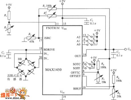
View full Circuit Diagram | Comments | Reading(989)
Pulse generator circuit using two complementary transistors
Published:2011/10/31 1:58:00 Author:May | Keyword: Pulse generator , two complementary transistors

It usestwo complementary transistorsto produce pointed pulse with theamplitude in 8V, rise time in 50nS+. This circuit pulse intermission is 1.4ms at the situation of charging capacitance is 10nF and 1M potentiometershort-circuited, and the weakening or decreasing capacitance value can make the pulse intermission increase or decrease. If 820Ω resistor isconnected at the emitter of NPN transistor instead of series with capacitor, it will get sharp pulse output.
(View)
View full Circuit Diagram | Comments | Reading(3887)
Square-wave generator circuit
Published:2011/10/31 2:00:00 Author:May | Keyword: Square-wave generator

T1 and T2 in the circuitform theinherent oscillator, T3 is output level. Network consists of high-pass filter (C3, C4, R6 + - R7) and low pass filter, it's output is added to the T3 base via C6 and R8, and in the collector of T3, it willget required square wave oscillation signal.
(View)
View full Circuit Diagram | Comments | Reading(1760)
The square-wave generator circuit with variable pulse width
Published:2011/10/31 2:06:00 Author:May | Keyword: square-wave generator , variable pulse width

The circuit uses theswitch Sto change the output pulse frequency range (20HZ ~ 20KHZ). Potentiometer RP1, rP2 are not only used for changing frequency, also can used to change pulse width. If changing RP2, RP1at the same time, it will only change frequency, the pulse width approximate remains unchanged. If only changing one potentiometer, it can form asymmetric positive or negative square wave signal. Diagram (b) shows a typical wave.
If the circuitbetween A, B, C in the diagram is replaced by diagram (C) , it can use RP1 to change duty ratio, use RP2 to change frequency. Here RP1 chooses >1MΩ, RP2 chooses 1MΩ, then it can get positive and negative sharp pulse output in low frequency.
(View)
View full Circuit Diagram | Comments | Reading(1821)
Crystal oscillator circuit using operational amplifier
Published:2011/10/31 2:07:00 Author:May | Keyword: crystal oscillator, operational amplifier

This circuit uses 761 operational amplifier, and theoutput pulse frequency can reach 10MHz. The 2KΩ resistor isused as operational amplifier output stage collector's load.
(View)
View full Circuit Diagram | Comments | Reading(2074)
The multivibrator circuit diagram with thyristor
Published:2011/10/31 2:14:00 Author:May | Keyword: multivibrator, thyristor

The circuit can produce 50V rectangular pulse, and its duty cycle T1 / (T1 + T2) canreach from 0.001 to 0.999 bycontinuously adjusting. This can be achieved by choosing the proper R3 and R5. Capacitor C1 and resistor R5can decide thefrequency, then the duty cycle is 50%.
(View)
View full Circuit Diagram | Comments | Reading(1508)
Simple sinusoidal oscillator circuit
Published:2011/10/27 21:13:00 Author:May | Keyword: sinusoidal oscillator

It can change the frequency range, and the oscillating signal is adjusted by potentiometer RP1. Since the output resistance is very low ( 1KΩ),it issuitable for various kinds of control circuit as a source.
In the circuit, the transistor's collector passesthrough R1, R2, C1, C2 to base to constitute feedback branch. Changing the device's parameters is OK.
(View)
View full Circuit Diagram | Comments | Reading(1871)
Threshold signal generator circuit using TcA965
Published:2011/10/27 21:19:00 Author:May | Keyword: Threshold signal generator

The circuit consists of multivibrator and threshold switch. The voltage of TCA965's pin 10 is decided by that of pin 6, pin 7, and pin 8, while the latter is determined by the bleeder R1~R4. The feedback is from pin 14 to pin 8 via R5. The unstable state occurs when the voltage of pin 9 is high enough. Then the circuit produces oscillation.
(View)
View full Circuit Diagram | Comments | Reading(2917)
Cheap solid amplifier circuit diagram
Published:2011/10/27 21:41:00 Author:May | Keyword: solid amplifier

μ voltage amplifying tube 6N1 (1/2) is made in the single-stage self-sufficient bias voltage amplifier with the gain K=20, when it is input 0.6V active voltage, it outputs 12V signal voltage to make the backward stage reach the specified output power 11W, which can definitely satisfy with each kind of sound source connection. The backward stage of power amplifier uses two 6P13P connected in parallel, which is used as the single-end Class A power output, and the loaded impedance is 1300Ω. Because the complete machine's distortion is not very high, therefore it will omit the negative feedback ring circuit to exhibit broad sound field. The 6P13P filament is supplied by AC 6.3V, and the 6N1 filament is supplied by the DC power supply. (View)
View full Circuit Diagram | Comments | Reading(2168)
Four-sound circulating burglar alarm circuit
Published:2011/10/27 21:52:00 Author:May | Keyword: Four-sound circulating, burglar alarm
When field-effect tube VT1 (3DJ6)'s wire is serviceable, it presents cut-off state, andpin 2 of JG (555) setting trigger end presents high level, and 555 is in reset state, namely pin 3 presents low level ( it islower than 0.4V). 555 and R1, C1 form the monostable trigger circuit. Whenpeople touch wire, human body's induction signal is amplified byVT1,set byIC1, thenits pin 3 turns to high level ( about 6V) to offer work voltage to IC2, VT2, etc.
When the wire is broken, IC1 is always in setting state, IC2, IC6, etc get electricity to be in continuous alarm state, and it send sout four- sound circulating alarm sound. IC2 and R2, R3, C4, etc make up ultra-low frequency multivibrator, and the oscillation or not depends on thepower supply. Its oscillation frequency f=1.44/(R2+2R3)C4. (View)
View full Circuit Diagram | Comments | Reading(890)
HD-3A energy-saving quota three-phase power supply protector circuit
Published:2011/10/27 22:12:00 Author:May | Keyword: Energy-saving quota , three-phase, power supply protector
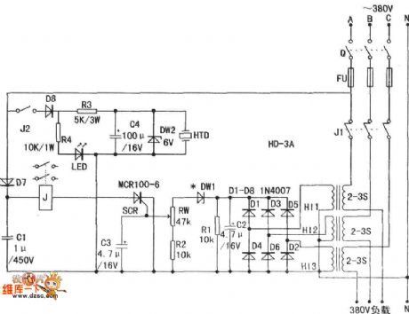
Current transformer H11-3can behomemade. People can choose transformer's iron core which is not less than 2W to wind secondaryfirstly.It usesΦ 0.12 mm varnished wire to wind1,000 turns. The primary uses Φ 1 ~ 4mm plastic wireto wind2 - 3 turns. It also can use current transformer. Finished current transformer induced voltage is quite high.
(View)
View full Circuit Diagram | Comments | Reading(2146)
Medium power linear amplifier pin circuit
Published:2011/11/2 21:02:00 Author:May | Keyword: power linear amplifier


RF2103P is thepower linear amplifier IC, which uses advanced GaAs heterojunction bipolar transistor (HBT), and it is designed for UHF frequency wireless transmit final linear RF amplifier, and its working frequency is 450~1000MHz. RF2103P also can be used as driver amplifier to applyin higher power situation, and the device includes power supply wire, bypass capacitor and matchingnetwork, and itcan generate 750mW (CW) output power. RF2103 can besupplied by 3 batteries, and the maximum CW is 175mW when output is 3.6V, and the device's total gain is 31dB. RF2103P can be used for digital communication system, spread spectrum communication system as high power linear driver. RF2103P pin array is shown in the picture.
Pin function is shown in the following diagram:
(View)
View full Circuit Diagram | Comments | Reading(621)
RF amplifier principle circuit composed of RF2103P
Published:2011/10/26 21:11:00 Author:May | Keyword: RF amplifier


RF signal (RF) isinput by pin 1, enlarged by preamplifier and final power amplifier ( FPA), thenoutput by pin 14. There is a blocking coupling capacitor between pin 1 and preamplifier, so it does not need to add coupling capacitor. Output ends pin 8, 9, 13, 14 are connected inside of the chip. Normally, pin 13, 14 are connected outside to be uses the as signal output, which connects to the matching network to make the amplifier output resistance match with it, then it gets themaximum output power and efficiency; and pin 8, 9 are connectedoutsideto beas power supply end, when it works at 915MHz, it adds a filter capacitor C2(=2pF) to ground tomake up filter circuitwith second harmonic, which can shortconnect second harmonic effectively.
(View)
View full Circuit Diagram | Comments | Reading(1179)
Multi-functional automatic charger circuit
Published:2011/10/26 21:17:00 Author:May | Keyword: Multi-functional automatic charger


The working principle is shown in Figure one. It is the controller with CD4060 being the core. CD4060 is the 14-bit binary serial counting/frequency divider and oscillator. It has two parts: one is the 14 levels of frequency divider, and its frequency division coefficient is 16-16384 (it is output by Q4,¯Q14). Another part is the oscillator, which may be the RC oscillator composed of the external connecting resistor and capacitor. f=1/2.2RT CT. It is shown in Figure two. This installment is the oscillator composed of the C4, R2, R3, and the frequency approximately is the 0.2Hz. LED2 is the bi-color light emitter diode.
(View)
View full Circuit Diagram | Comments | Reading(2260)
Panasonic KY-P2N microwave cooker principle diagram
Published:2011/8/29 22:50:00 Author:Jessie | Keyword: Panasonic , microwave cooker
View full Circuit Diagram | Comments | Reading(2572)
Medium power amplifier RF2104 pin circuit
Published:2011/10/26 21:27:00 Author:May | Keyword: Medium power amplifier

RF2104 is the medium power amplifier IC, and the design is used in UHF frequency band radio transmitting last stage linear RF enlarging, and the operating frequency is 400~1000MHz. RF2104 can be used as the driver amplifier to apply in the high power situation, and it uses the square bat-flyaway 16-lead seal. RF2104 can be supplied by 3-battery power supply, and the biggest CW output is +27dBm when the power is 3.6V, the component overall gain is 26dB. RF2104 is used in 900MHz ISM frequency band, 400MHz industry radio traffic, high-power driver, portable battery supply set, commercial and the consumer system, base depot equipment and so on. (View)
View full Circuit Diagram | Comments | Reading(796)
DPCA Picasso 1.6 L car ABS circuit diagram
Published:2011/8/29 22:38:00 Author:Jessie | Keyword: DPCA Picasso , 1.6 L car, ABS

View full Circuit Diagram | Comments | Reading(1063)
Passat 01N automatic transmission circuit
Published:2011/8/30 1:48:00 Author:Jessie | Keyword: Passat , automatic transmission

View full Circuit Diagram | Comments | Reading(1456)
| Pages:389/2234 At 20381382383384385386387388389390391392393394395396397398399400Under 20 |
Circuit Categories
power supply circuit
Amplifier Circuit
Basic Circuit
LED and Light Circuit
Sensor Circuit
Signal Processing
Electrical Equipment Circuit
Control Circuit
Remote Control Circuit
A/D-D/A Converter Circuit
Audio Circuit
Measuring and Test Circuit
Communication Circuit
Computer-Related Circuit
555 Circuit
Automotive Circuit
Repairing Circuit