
Circuit Diagram
Index 381
Precision photoelectric detection isolated amplifier ( ISO212 ) circuit
Published:2011/8/31 1:50:00 Author:Jessie | Keyword: photoelectric detection , isolated amplifier

The circuit adopts jfetinput integrated amp OPA128. This amp has very low offset current, which is about 40~150fA (1fA=10-15A),so its input impedance is extremely high (is about 1013//lΩ//pF), it andphotoelectric diode BPW21 form the photoelectric detection circuit with excellent performance. The photoelectric detection circuit will change light signals into electrical signals, andit issent to photoelectric coupling isolated amplifier ISO212P after amplifing,and that is the photoelectric detection isolated amplifier. (View)
View full Circuit Diagram | Comments | Reading(2046)
4~20mA current transmitter circuit with digital pressure signal disposal device MAX1459
Published:2011/8/31 1:47:00 Author:Jessie | Keyword: current transmitter, digital pressure signal disposal device
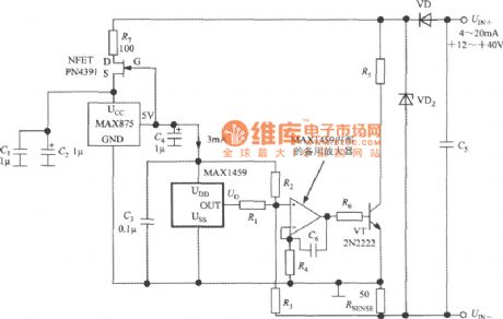
PGA's output voltage is sentto spare amplifier in chip, then we can get 4~20mA output current by external power amplifier circuit. In long-distance transmission current, the current signal's precision is not influenced by the resistance of cable. PN4391 is a 40V, 150mANFET. MAX875's voltage temperature coefficient is 7×10⁻⁶/℃. The 3mA constant current source iscomposedof PN4391 and MAX875, and it provides stable work current to MAX145, then it uses MAX1459 to take temperature compensation and gain compensation. MAX1459's output voltage is converted into 4 ~ 20mA current signal through backup amplifier and power amplifier, and its loop power range is + 12 ~ 40V. VT uses 2N2222 power tube, and its main parameters are: UCEO = 60 V, ICM = 0.8 A. The initial voltage of measuring resistance is set by resistors R1 ~ R 4, and the signal voltage of RSENSE is controlled by MAX1459. (View)
View full Circuit Diagram | Comments | Reading(2324)
Photoelectric receiving amplifier circuit with LM307
Published:2011/8/30 22:28:00 Author:Jessie | Keyword: Photoelectric receiving amplifier

Photoelectric receiving amplifier is used to magnify photoelectric diode or light activated triode's output signals. When the light intensity of incident lightchanges, photodetector will produce corresponding voltage or current, and photoelectric receiving amplifier is used to amplify the photo-current changes, photoelectric receiving amplifier circuit with LM307 is the ideal device to realize the above role. If it adds offset voltage VB on light activated triode OS18, its output current in the illumination is Vo=IpR1. The photo-current Ip'sminimum is determined by LM307's input amplifier drift IB, Ip's maximum is determined by the maximum voltage output Vomax. (View)
View full Circuit Diagram | Comments | Reading(1571)
Temperature measuring system circuit box circuit with thermocouple cold end temperature compensation and converter MAX6675
Published:2011/8/30 22:12:00 Author:Jessie | Keyword: Temperature measuring system, circuit box, thermocouple cold end temperature compensation, converter

The temperature measuring system composedof MAX6675 is shown in the diagram. K thermocouple is connected to the T+ and T- of MAX6675, and the cold endof thermocouple is in the ground. Host chooses the 8051 microcontroller, and MAX6675 is the slave. From the P1.1 port of 8051, it sends serial clock to MAX6675,and P1.0 portis used to receive MAX6675 output temperature data. P1.2 port outputs low level to set CS 0. System is equipped withfive-position common cathode LED digital tube. Set decimal pointat ten behind, then wecan measure the temperature of 0~ +1024 ℃, and resolution is 0.1 ℃. P0 port is used to respectively connect decoding drive CD4511 and driver 74LS154. (View)
View full Circuit Diagram | Comments | Reading(1651)
Detection thermocouple open-circuit fault(isolated thermocouple cold compensation and signal conditioner 1B51) circuit
Published:2011/8/30 21:50:00 Author:Jessie | Keyword: Detection thermocouple, open-circuit fault, isolated thermocouple , cold compensation , signal conditioner

View full Circuit Diagram | Comments | Reading(1194)
Temperature measurement instrument circuit with thermocouple cold end temperature compensator AD596/597
Published:2011/8/30 21:45:00 Author:Jessie | Keyword: Temperature measurement instrument, thermocouple cold end temperature compensator
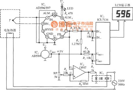
AD596/597 is used as a closed-loop thermocouple signal disposal implement. IC2 is CMOS monolithic 3 1/2 A/D converter ICL7136,which can be replaced byusing ICL7106, but power consumption will increase a little. IC3 is +5V bandgap benchmark voltage source AD584, +5V benchmark voltage provides1.000V benchmark voltage to ICL7136 after separated voltage by R4, R5, DPMwith full range in 2V is composedof ICL7136 and LCD display. IC4 chooses OP07 operational amplifier. RPis a setting point adjust potentiometer, which is used to set the controlling temperature T1. IC5 is TRIAC's optical coupler. (View)
View full Circuit Diagram | Comments | Reading(2369)
Digital pressure signal disposal device MAX1458 bridge excitation circuit
Published:2011/8/31 1:51:00 Author:Jessie | Keyword: Digital pressure signal disposal device, bridge excitation

Digital pressure signal disposal device MAX1458 bridge excitation circuit is shown in figure. Using DAC3's outputcan change sensor incentive current IBR's value, then itwillrealize full range fine calibration. IISRC is benchmark current, and it is set by the voltage of RISRC and pin 9. V1 and V2form mirror current sourcem, current gain is 14 times, and it can make incentive current IBR=14IISRC. IBR's programming rangeis 0.1~2mA. Analog switches S1, S2's hige state is controlled by configuration register. Obviously, when full range output voltage changes, DAC3 will compensate bridge road output voltage by changing BR, and correct full range error. DAC4 is used tocorrect full range temperature coefficient error. (View)
View full Circuit Diagram | Comments | Reading(617)
Digital electric clock circuit diagram
Published:2011/8/30 1:56:00 Author:Jessie | Keyword: Digital electric clock


As shown in figure, digital electric clock circuituses electronic horologe special integrated circuit KD482FCas seconds time-base signal. Through the digital circuit multi-stage separate frequency, it formsminute and hour to output. The minute isdisplayed byLED digital tube; While hour display is the analog dial structure of mechanical pointer clock,and itis displayed by light-emitting diodes in the dial. It's timing accurately, novelly, so it is very suitable for amateur toimitate. The circuit is composedof thesecond time base signal form circuit, minute time formation-display circuit and the hour formation-display circuit. (View)
View full Circuit Diagram | Comments | Reading(1570)
Triple-digit display electronic timer circuit composed of NE555 and CD40110
Published:2011/8/30 1:58:00 Author:Jessie | Keyword: Triple-digit display , electronic timer

As shown in figure is electronic timing which is used for raider type cars. Car startups will launch timer,while car stops makes the timer stop.The value that car showsis the racing spending time. This circuit is composedof thecontrol switch and electronic timer. And electronic timerconsists of the time base generator and digital electronic counter. (A)is principle diagram; (b)is control switch circuit. IC1, IC2 and IC3are CD40110. (View)
View full Circuit Diagram | Comments | Reading(3291)
Countdown display timer circuit with NE556, CD40110
Published:2011/8/30 2:01:00 Author:Jessie | Keyword: Countdown display timer

Digital display countdown timer can make people always see how much time left, it has certain practical value to some applications. As shown in figure, itis a digital display timing circuit, its structure is simple, and is easy to make. Its time-base unit adjustable. This circuit uses harmonic oscillator, which is composedof NE555 circuit as time base. Although the time precision is not quite high, it is economical and suitable. Full circuitis composedof adjustable time base signal generator, minus count, display and output signal control circuit etc. (View)
View full Circuit Diagram | Comments | Reading(3627)
Phone minute beep decoder circuit with NE555, CD4017
Published:2011/8/30 2:09:00 Author:Jessie | Keyword: Phone minute beep, decoder
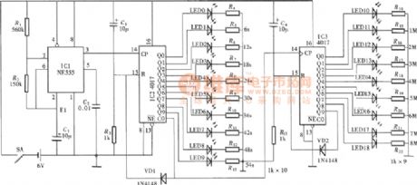
At present, our country telephone is executed with method of using minute as timing charging unit, except the charging in the first 1 min. Namely, the first time is fixed charging. Whenever enter the next time, the first 1s will immediately add the one-time charging. For the longer time's call speaking, the over 1 min should be paid low proportion in the whole conversation. But to those calls which often finished in the 1 min, even talk time delays 1 s, the over fee's proportion is high in the whole fee. The timing remind decoder circuit is shown as the chart. Full circuit is composed of the 6s time-base generator, 6s separate-frequency timing display and minute timing display. (View)
View full Circuit Diagram | Comments | Reading(4193)
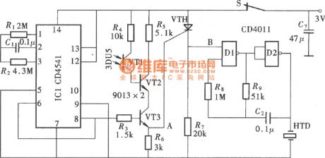
Open/stop selecting function timer circuit with CD4541
Published:2011/8/30 2:11:00 Author:Jessie | Keyword: Open/stop selecting function, timer

CD4541 is the main partof the timer. It can chooseto open firstly, or stopby switch. In circuit, timing time's adjustment is choosing by switch,the amount of the resistance between CD4541's pin1 and pin 2increasing and decreasing. Because resistance is decided as first, every resistoris fixed. So it is more convenient and accurate than the potentiometer to adjust timing time.The Circuit is composedofthe open/stop preset circuit, adjustable open/stop timing circuit, output control and executing circuit. (View)
View full Circuit Diagram | Comments | Reading(5506)
Division circuit with NE555
Published:2011/8/30 2:13:00 Author:Jessie | Keyword: Division

The circuit as shown is composedof thevoltage-frequency converterand amplitude modulator. Input V1 controls the resistance of mosfet 2N4222 by operational amplifier A1. Soit can change the oscillation frequency of no steady-state much harmonic oscillator. A2 is an input signal amplitude modulator. The input signal V2 is output after being modulated.It setsthe clip broken voltage of mosfetas Vp, if (1+R1/R2)=Vp, then the relationshipbetween output and input is: Vo=-V2/V1. The range of V1 and V2 is 0~10V. Output Vo is an average value, which can be gotten from filter or damping type voltmeter. (View)
View full Circuit Diagram | Comments | Reading(1223)
Medication regularly remind decoder circuit with CD4541
Published:2011/8/30 2:15:00 Author:Jessie | Keyword: Medication, remind decoder
Medication regularly remind decoder is designed for those sicks who needs constantly medication. This reminder can be installed on family special medicine box, and it sets timer intervals according to the number of taking medicine everyday. When arrived at the scheduled time, reminder sounds. After openning medicine box, the sound stops and enters the nexttiming interval. This circuit is composedof the timer, remind audio generator and related control circuit. (View)
View full Circuit Diagram | Comments | Reading(4675)
Circulation regularly reminded decoder circuit with CD4511
Published:2011/8/30 2:20:00 Author:Jessie | Keyword: Circulation regularly reminded decoder

It uses two CD4541 connected in series to compose a circulation timer. The output terminal connected a sound circuitto form a regularly reminder circuit. This regularly reminder circuit has many uses, such as for the patient's care, regularly reminded medication, etc. Reminding sound circuit can be chosenaccording topeople's favoritemusic integrated circuit. This timer chooses musical CW9300 as sound circuit,and itscomposition is as shown. (View)
View full Circuit Diagram | Comments | Reading(2019)
Hafei Simbo car charcoal canister electromagnetic valve circuit diagram
Published:2011/8/30 1:33:00 Author:Jessie | Keyword: Hafei Simbo car, charcoal canister, electromagnetic valve

View full Circuit Diagram | Comments | Reading(1290)
Wanhe ZLD-72 computer control horizontal electronic alexipharmic ark circuit
Published:2011/8/30 1:34:00 Author:Jessie | Keyword: computer control, horizontal, electronic alexipharmic ark
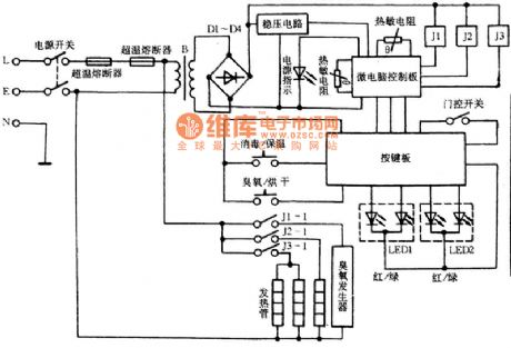
View full Circuit Diagram | Comments | Reading(2300)
The voltage-dividing bias amplifier circuit diagram of mosfet
Published:2011/8/24 2:21:00 Author:Jessie | Keyword: voltage-dividing bias amplifier, mosfet

View full Circuit Diagram | Comments | Reading(1049)
Common emitter amplifying circuit
Published:2011/8/24 2:19:00 Author:Jessie | Keyword: Common emitter, amplifying

Common emitter amplifying circuit
The amplifier's role: amplifiering faint signals (voltage, current, and power) to the required category. The role of each element: Transistor T-- The amplification component, iC = b iB. It must ensure the collector junction reverse bias, the emitter biased to make the transistor work in the enlarged area. Base power EB and base resistor RB-- Make emitterforward bias, and provide the proper size base current. Collector power EC-- Provide the energy for the circuit. And guarantee BC junction reverse bias. The collector resistance RC-- Change current amplification to voltage amplification. Coupling capacitors C1, C2--theyisolate input, output and amplifying circuit DC's link to beAC signal input and output smoothly. (View)
View full Circuit Diagram | Comments | Reading(1138)
Nianfeng YWQ-900 automatic electric pressure cooker circuit
Published:2011/8/24 2:16:00 Author:Jessie | Keyword: automatic electric pressure cooker
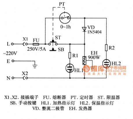
X1, X2-plug terminals, FU-fuse, PT-timer, ST-limit thermostat, SB-hand button, HL1-heating lamp, HL2-heat indicator, VD-rectifier diode, EH-heater (View)
View full Circuit Diagram | Comments | Reading(1652)
| Pages:381/2234 At 20381382383384385386387388389390391392393394395396397398399400Under 20 |
Circuit Categories
power supply circuit
Amplifier Circuit
Basic Circuit
LED and Light Circuit
Sensor Circuit
Signal Processing
Electrical Equipment Circuit
Control Circuit
Remote Control Circuit
A/D-D/A Converter Circuit
Audio Circuit
Measuring and Test Circuit
Communication Circuit
Computer-Related Circuit
555 Circuit
Automotive Circuit
Repairing Circuit