
Circuit Diagram
Index 391
Operational amplifier attenuation circuit diagram
Published:2011/8/19 2:15:00 Author:Jessie | Keyword: Operational amplifier, attenuation


Reversed-phase composedof op-amp attenuator is shown in figure 1 . In the circuit, R2 is less than R1. This method is not recommended, because many op-ampsare not suitable for the working condition ofthe magnification whichis less than 1. Accurate method is to use figure 2 circuit. In table 1, a set of normalization of R3 resistor can be used to produced different level attenuation. The other resistors can use the following formula: R3=(Vo/Vin)/(2-2(Vo/Vin)). (View)
View full Circuit Diagram | Comments | Reading(973)
YS-608 Learning headset principle and maintenance circuit
Published:2011/8/24 2:30:00 Author:Jessie | Keyword: Learning headset, principle, maintenance

The headset circuit entirely composedof division components. When single pole double throw switch K is dialled to 1 position, the headset is at the state ofreceiving infrared, thereceiver tube will receive infrared speech signal from 100 parallel infrared emitting tubes which are in the back of the classroom. This signal is coupledfrom the capacitor C1 to Q1 to amplify, then the voice signal issent to the two level percentile amplifier circuit which is composedof Q2, Q3, and promote left/right two parallel headsets togive off sound. (View)
View full Circuit Diagram | Comments | Reading(754)
Children anti-lost reminder circuit
Published:2011/10/24 1:35:00 Author:May | Keyword: Children anti-lost reminder
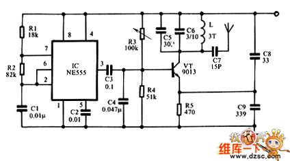
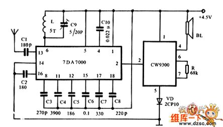
Figure 1 shows the transmitter circuit. It consists of time-base IC NE555, R1, R2, C1. 1KHz low-frequency oscillator can modulate the high-frequency oscillator composed of transistor VT and peripheral components, then the modulated high-frequency signal is sent out by the inside tiny antenna from the C7. C8 is used to add broadband and prevent impact on the frequency from human induction. Actual use proves that it is the essential element. Figure 2 shows the receiver circuit. When the receiver receives the signal sent by the transmitter, the pin ② of IC TDA7000 outputs low level, the music IC CW9300 has no high level to trigger signal and does not work, then speaker BL is silent.
(View)
View full Circuit Diagram | Comments | Reading(2659)
Operational amplifier virtual earth circuit
Published:2011/8/24 2:29:00 Author:Jessie | Keyword: Operational amplifier, virtual earth

The op-amp of single-voltage's work requires to provide a virtualfor external, of whichvoltageisnormally VCC/2. In graph 2, thecircuit can be used to produce the VCC/2 voltage, butit will reduce the system frequency characteristics. R1 and R2are equivalent, which is choosen through the consumption and noise, and capacitorC1 is a low-pass filter, which is used to reduce the noise coming from power. In some applications,buffer op-amp can be ignored. (View)
View full Circuit Diagram | Comments | Reading(1012)
High-efficiency high power amplifier RF2131 pin circuit diagram
Published:2011/10/24 2:06:00 Author:May | Keyword: High-efficiency, high power, amplifier

RF2131 is high-power and high-efficiency amplifier. It adopts advanced GaAs hetero-junction bipolar transistor technology. It is designed for final linear RF amplifier of ETACS handheld device, CDPD, band spread system and other applications with working frequencyin 1800~2500MHz. It offers an analog voltage input end with power control rangein 30dB. The power supply decreases when it is in the logic low-level state. And, the power supply is in the spare working state. It is designed for C class, but it can work at linear AB class if itimprove bias voltage. The device itself includes 50Ω input and output. So it is very easy to match best power and efficiency features. RF2131 is used for AMPS/ETACS cellular system mobile phone, CDPD portable data card, 900MHz ISM frequency range device, commercial and consumer systems, portable battery power supply unit, etc. The pin array of RF213 is shown in the diagram.
(View)
View full Circuit Diagram | Comments | Reading(895)
Wireless motorcycle burglar alarm circuit
Published:2011/10/24 2:32:00 Author:May | Keyword: Wireless, motorcycle burglar alarm
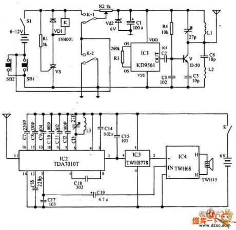
The relay K and SCR VS are used to control the transmitter circuit's power. IC1 forms the alarm signal circuit. And the transistor V and its peripheral components form the radio frequency oscillator circuit to transmit alarm signal. In the waiting state, the switch S1 is connected, and SB1 is disconnected (ie, the front lock is locked), K is in the release state, then the alarm transmitter does not work. When the lock is opened (ie SB1 is connected), VS is triggered for conduction, K is pulled in to turn on the transmitter power. SB1 is switched on, K-2's normally open point is self-locking, and only alarm S1 disconnecting can end the alarm at this time. When K acts, its normally closed contact K-l is off.
(View)
View full Circuit Diagram | Comments | Reading(1383)
The best efficiency power amplification circuit of RF2131 with 4.8V power
Published:2011/10/24 2:39:00 Author:May | Keyword: best efficiency, power amplification , 4.8V power

RF signal (RF) is input by pin 7, and it is output by pin 10, 11, 14 and 15 after enlarging by preamplifier and final stage power amplifier. Pin 7 is directly coupled with internal amplifier. So pin 7 is added a blocking coupling capacitor. The input impendence of pin 7 is 50Ω, but the precise resistance is determined by out connected internal matching network of pin 3. Pin 10, 11, 14 and 15 of output endare connectedto the chip. Normally, pin 10. 11, 14 and pin 15are separately connected together and used as signal output.People must pay attention to symmetry. In order to get largest output power and efficiency, output matching network can make amplifier's output impendence match with it. At the same time, the pins are also used as final power amplifier's power supply end. It offers bias current to final operation amplifier through the pins. (View)
View full Circuit Diagram | Comments | Reading(669)
TV lightning protection circuit
Published:2011/10/26 22:14:00 Author:May | Keyword: TV lightning protection
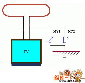
The application circuit of this set is shown in the picture. Watching TV on in thunderstorms, the thunderbolt can scurry into TV and damage it through two ways; one is through outdoor television antenna; the other is through TV power line. The former often damages radio-frequency head, the latter often damages TV power supply circuit and line-field output circuit. Adding voltage dependent resistor on outdoor antenna can avoidthe consequence, and itrequires voltage dependent resistor MY to beconnected with ground directly. Protective power supply part application circuit's connectioncan be seen in the picture. They general protect induced lightning, if it meets the direct lightening, because of thedirect lightening's huge current and extreme high voltage, voltage dependent resistor cannot do anything about it, so we should place lightning conductor around outdoor antenna, the position of outdoor antenna should bein the protected areas.
(View)
View full Circuit Diagram | Comments | Reading(1928)
RF2132 Dual-mode high-power linear amplifier pin diagram
Published:2011/10/24 2:42:00 Author:May | Keyword: Dual-mode, high-power, linear amplifier

RF2132 is a high power and efficiency linear amplifier. It is treated by advanced GaAs hetero-junction bipolar transistor. And it is designed for the final linearity RF amplification of double mode four battery's CDMA/AMPS handheld digital cellular system equipment, band spread system and other applications with working frequency 800~950MHz. The device itself includes 50Ω input and output. So it is very easy to match and get best power, efficiency and linear property when the whole power supply and control voltage changes. FR2132 is used in 4.8V AMPS cellular systems mobile phone, CDMA/AMPS mobile phone, JCDMA/TACS mobile phone. It can also beused as driver amplifier, portable battery supplyin the base station. The pin array and functions of RF2132are shown in the diagram.
(View)
View full Circuit Diagram | Comments | Reading(848)
Keyer dimmer table lamp circuit
Published:2011/10/26 20:58:00 Author:May | Keyword: Keyer, dimmer table lamp

Keyer dimmer table lamp adopts two touch buttons to adjust the light. The light changes weaken from strong when peopletouch one of the buttons, and it changes strong from weaken when peopletouch the other button.
Working principle
The principle of this circuit is shown in diagram 1. Capacitance buckDC power supply is composed of VD1, VD2, C2 and C3. Triac VS's trigger circuit is composed of MOSFET, C1 and so on. DW is protecting diode. It can prevent the grid breakdownfrom FET. When people press down S1, R1 charges to the C1 to increase the grid bias, then the silicon-controlled rectifier's trigger current rises, the breakover angle increases, the optical fiber increases; when people press down S2, C1 discharges along the R2, the grid bias drops, silicon-controlled rectifier's breakover angle lessens, the optical fiber changes darker. (View)
View full Circuit Diagram | Comments | Reading(2978)
Linear power amplifier circuit composed of RF2132
Published:2011/10/24 2:50:00 Author:May | Keyword: Linear power amplifier

The diagram is linear power amplifier circuit composed of RF2132. Radio-frequency signal (RF) isinput by pin 3, enlarged by preamplifier and final power amplifier, then output by pin 10, 11. Pin 3 is directly coupling with internal amplifier, and it is added a blocking coupling capacitor, and the input resistance of pin 3 is 50Ω, but the precise resistance is determined by interstage matching network connected to pin 1. L1 is output center frequency level adjusting inductance; R1 can improve linearity, add first level ampliifer current bias; L2 is amplifier output stage bypass inductor. Output ends pin 10, 11, 14, 15 are connected to the chip. Pin 8 is connected topower control foot (PC) to control this pin voltage and power. At room temperature, when voltage is inlow level ( when it is 0.5V or lower) , amplifier power is on the shutoff state. Vcc=4.8V, Vpc=4.0V.
(View)
View full Circuit Diagram | Comments | Reading(1123)
T1A-14 vacuum tube one-port class A amplifier-headphone amplifier amphibious circuit
Published:2011/8/29 20:57:00 Author:Jessie | Keyword: vacuum tube, one-port class A amplifier, headphone amplifier, amphibious circuit

View full Circuit Diagram | Comments | Reading(2702)
M6 car automatic transmission circuit diagram
Published:2011/8/29 20:58:00 Author:Jessie | Keyword: car automatic transmission

View full Circuit Diagram | Comments | Reading(655)
2a3 tube amp circuit diagram
Published:2011/8/29 21:17:00 Author:Jessie | Keyword: tube amp

View full Circuit Diagram | Comments | Reading(3118)
Bravery machine amplifier pins circuit diagram
Published:2011/8/24 2:39:00 Author:Jessie | Keyword: Bravery machine, amplifier pins

View full Circuit Diagram | Comments | Reading(638)
Buick GL8 car ABS wheel speed sensor and ABS electronic control unit circuit
Published:2011/8/24 2:38:00 Author:Jessie | Keyword: Buick GL8 car, ABS wheel, speed sensor, ABS , electronic control unit
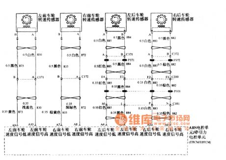
Buick GL8 car ABS wheel speed sensor and ABS electronic control unit traction electronic control unit EBCMEBTCM circuit (View)
View full Circuit Diagram | Comments | Reading(917)
Banqiu HE-2700E1, HE-2700E2 temperature-regulating electric furnace circuit diagram
Published:2011/8/29 22:37:00 Author:Jessie | Keyword: Banqiu, temperature-regulating , electric furnace

ST1, ST2-thermostat, HL1.HL2-light, EH1, EH2 heater
(View)
View full Circuit Diagram | Comments | Reading(710)
Banqiu CCDT5-4 electronic thermostat electric-fry pan circuit diagram
Published:2011/8/29 20:53:00 Author:Jessie | Keyword: Banqiu , electronic thermostat , electric-fry pan
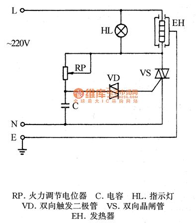
RP-fire adjustment potentiometer, C-capacitor, HL-light, VD-way trigger diode, VS-Triac, EH-heater.
(View)
View full Circuit Diagram | Comments | Reading(2032)
Meifeng DYB40-80A insulation automatic electric pressure cooker circuit
Published:2011/8/24 2:37:00 Author:Jessie | Keyword: insulation, electric pressure cooker

XB-power connector, FU-fuse, PT-timer,EH1,EH2-heater,led1-power indicator, LED2-heater indicator, LED3-heater lamp (View)
View full Circuit Diagram | Comments | Reading(689)
Jiabao YWB-55 automatic electric pressure cooker circuit
Published:2011/8/24 2:33:00 Author:Jessie | Keyword: electric pressure cooker

FU-Fuse, T-power transformer, ST1, ST2-thermostats, PT-timer, K1-relay, K1-1 normally open contact of relay K1, K1-2-relay normally closed contact of K1, HL1-heat indicator, EH1, EH2-heaters (View)
View full Circuit Diagram | Comments | Reading(1051)
| Pages:391/2234 At 20381382383384385386387388389390391392393394395396397398399400Under 20 |
Circuit Categories
power supply circuit
Amplifier Circuit
Basic Circuit
LED and Light Circuit
Sensor Circuit
Signal Processing
Electrical Equipment Circuit
Control Circuit
Remote Control Circuit
A/D-D/A Converter Circuit
Audio Circuit
Measuring and Test Circuit
Communication Circuit
Computer-Related Circuit
555 Circuit
Automotive Circuit
Repairing Circuit