
Circuit Diagram
Index 380
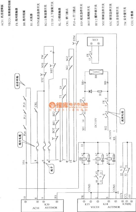
Beijing fuerrui elevator safety loop and band-type brake circuit
Published:2011/8/24 2:46:00 Author:Jessie | Keyword: Beijing fuerrui , elevator safety loop, band-type brake
View full Circuit Diagram | Comments | Reading(1027)
Matsushita L15 power supply
Published:2011/12/5 1:21:00 Author:May | Keyword: Matsushita, power supply

The model number of TV which using Matsushita L15 power supply have: TC2171, TC2173, TC2185, TC2186, TC-D21, TC-D25, etc. Main switch power supply consists of STR50213 which belongs to series stabilized voltage supply.
Oscillation circuit
Q834 is 113V overvoltage protection circuit. When 113V is normal, Q834 is cut off. If 113V is too high, Q834 is turned on. If 113V is in short circuit, the oscillation stop.
APS and remote control shutdown circuit
When the TV is normally starting, CPU’s pin 6 outputs high level. It will make Q814 turn on. At this time, Q810, Q811, Q812, Q813 are all cut off. And APS is not working. (View)
View full Circuit Diagram | Comments | Reading(1697)
Separate excitation switching regulated power supply 2
Published:2011/12/5 1:19:00 Author:May | Keyword: Separate excitation, switching regulated power supply

The diagram is theseparate excitation switching regulated power supply circuit which uses single-junction transistor as pulse generator. VDl ~ VD4 and C1form rectifier filter circuit, it can change 220V AC mains voltage into 300V DC voltage. Pulse generator consists of single junction transistor VT1, resistors R3, R4, R5, potentiometer Rp and capacitor C3. And changing the resistance of the potentiometer Rp can change the pulse frequency. C4 is coupling capacitor of output pulse. R1 and R2 can divide 300V DC voltage and send 20~30V working voltage of single junction transistor VT1. VT2 is inverting amplifier tube. It can invert andamplify positive polarity pulse output by pulse generatorand send negative polarity pulse to switching tube VT2, it can make itself cut off when VT1 outputs positive polarity pulse.
VT3, R7, C5 make up protection circuit of switching tube VT4. (View)
View full Circuit Diagram | Comments | Reading(1761)
Push pull type switching regulated power supply principle diagram
Published:2011/11/21 21:15:00 Author:May | Keyword: Push pull type, switching regulated power supply

Push-pull converter circuit belongs to double-ended type conversion circuit. Its high-frequency transformer works atboth sides of the hysteresis loop. The typical circuit is shown as the chart. Switching transistors VT1, VT2 are alternately turned on and off after inspiring by base driving circuit, the input DC voltage Ui is converted into high frequency square wave AC voltage. When VTl is turned on, Ui is added to the primary winding N1 of the transformer T1 by VT1. When the base incentive disappears, VTl, VT2 tubes are closed. The collector voltage is input voltage Ui. Next half cycle, VT2 is turned on, VTl is ended, VT1 can add two times input voltage, after the two tubes cut off, and the next cycle is started again. The main disadvantage of push-pull circuit isthat switching transistor voltage should reach 2 times of input power. To take 220 ± 10% V grid voltage for an example of peak voltage, the maximum steady state cutoff voltage is 680V. (View)
View full Circuit Diagram | Comments | Reading(1703)
Practical circuit of push-pull converter type switching regulated power supply
Published:2011/11/21 21:20:00 Author:May | Keyword: push-pull converter type, switching regulated power supply

The diagram shows a practical circuit of push-pull converter type switching regulated power supply. CW494 is double-ended converter modulator integrated circuit which includes error amplifier, voltage reference, clock oscillator, pulse width modulator and other circuits. Transformer T1 is high-frequency transformer which can transfer energy to the load. T2 is incentive promotion transformer. It can transmit two strings of pulse modulator outputted by CW494 pulse modulator to drive and switching tube base of push pull circuit after it enlarged through incentives promote transistor. Winding transformer T3 is the sampling pulse of AC voltage on the transformer and rectified through by the sample sent to the pulse modulation circuit resistance CW494 16 feet, as the error amplifier inverting input.
The selection of power switching power transistor is fast series F461. In the place where the voltage is feedback, input and output are directly connected. If the input and output need to be isolated, the optocoupler can be used. (View)
View full Circuit Diagram | Comments | Reading(1612)
Output sampling winding isolated switching power supply
Published:2011/11/22 0:07:00 Author:May | Keyword: Switching power supply, output sampling, winding isolated

The diagram shows the output sampling winding isolated switching power supply . In diagram, T is high frequency transformer; N2 is self-oscillation positive feedback winding; N3 is the error amplifier , and VTSis thewinding to provide sampling signal; N4, N5are DC output windings. DC output and the power gridare isolated from each other, because N3, N4, N5 are isolated from each other.
The power supply has two sets output of 6.3V and 100V DC. 35V voltage is used in error amplifier.
When output voltage is increasing, the sampling resistor’s voltage UD is increasing, error amplifier VT3’s collector current is increasing. Positive partial voltage offered to variable resistance tube VT2 by voltage drop of resistor R8 generated by the current is increasing, so that the collector current of VT2 is increasing.
The voltage dropping Ucd2 is reduced to be equivalent to the shunt resistor between base of switching tube VT1 and ground. (View)
View full Circuit Diagram | Comments | Reading(2772)
Dual output switching regulated power supply
Published:2011/11/22 0:47:00 Author:May | Keyword: Dual output, switching, regulated power supply

The circuit diagram of 15W switching regulated power supply with +5V (3A) main output and +3.3V (0.1A) alternative output is shown in the following diagram. This power supply adopts one piece of TOP223Y type single chip switching power supply with TO-220 packaging. Its maximum output power is 30W. It can use the power supplyfor printer and monitor. If the main power supply is +3.3V, it can be used for the switching power supply of notebook. The input voltage range of this power supply is 85~265V. The voltage regulation factor is ±0.7%, load regulation factor is +1.1%, power supply efficiency η>70%.
The features of this power supply is shown in the following: (1) it can output +5V, +3.3V two loads isolation stable voltage at the same time; (2)It can further improve the stability of _5V and +3.3V output voltage to add one piece adjustable precision parallel voltage regulator IC3 (TL431) ; (3)it adds RC absorb circuit composed of C11, R7 to eliminate high frequency self-oscillation and decrease radio frequency interference (RFI). (View)
View full Circuit Diagram | Comments | Reading(3100)
Boost chopping type switching stabilized voltage supply principle diagram
Published:2011/11/22 0:44:00 Author:May | Keyword: Boost, chopping type, switching stabilized voltage supply

The diagram is boost chopping type switching stabilized voltage supply principle diagram. When switching component is controlledto besaturation conduction, the current passing inductor to make it store energy. When switching component VT is controlled and in the cut-off state, the energy stored in inductor still offers to load through diode VD, meanwhile it is charging to capacitor C. When load voltage is dropping down, the capacitor is discharging again. At this time, it can get stable voltage which is higher than input voltage. It is also called parallel switching stabilized voltage supply, because switching component VT and load resistor RL is parallel. (View)
View full Circuit Diagram | Comments | Reading(744)
Boost and output practical circuit
Published:2011/11/22 0:42:00 Author:May | Keyword: Boost, output, practical
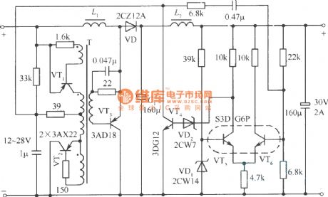
The diagram is a boost andoutput practical circuit. VT3 is switching regulating tube. Regulation tube VD2 can convert the potential. VT4 is paraphrase isolation amplifier. VT4 and its load which is 33kΩ resistor will divide the voltage Ui. The two voltages are separately provided to impulse generator. Impulse generator consists of transformer T and VT1, VT2. This is free running multi-vibrator of asymmetric transformer positive feedback. The power of VT1 comes from the voltage on 33kΩ resistor. The current on resistor depends on the current of VT4. The power supply voltage of VT1, VT2 is different. Each half period oscillation amplitude changes in direct proportion, the width changes in inverse proportion. Then it can control the turn-on and cut-off time. When output voltage is increasing, the current of differential pair tube VT6 of error amplifier is decreasing, collector potential is increasing, 33kΩ resistor up voltage drop is enlarge, VT1 tube power supply voltage is increasing, the turn on time is shortening, switching tube VT3’s turn on time is shortening.
The input voltage of this circuit is 12~28V, the output can be stabilized at 30V, the maximum output power is 60W, the efficiency is 88.9%~94.7%, the instability degree is ±0.33%, the output voltage ripple factor is 0.02&, the working frequency is 10kHz.
(View)
View full Circuit Diagram | Comments | Reading(1043)
Practical circuit of zero current switching soft switching stabilized voltage supply
Published:2011/11/21 20:50:00 Author:May | Keyword: zero current switching, soft switching, stabilized voltage supply

The diagram is a practical circuit ofzero current switchingsoft switching stabilized voltage supply. Its input is single phase alternating current. Its output is direct current. The main switching tube adopts MOSFET. Power switching circuit adopts half bridge circuit. Integrated control chip uses UC2865. Its power switching mode adopts zero current switching circuit.
(View)
View full Circuit Diagram | Comments | Reading(1607)
Frequency modulation type switching stabilized voltage supply 1
Published:2011/11/22 0:27:00 Author:May | Keyword: Frequency modulation, switching, stabilized voltage supply

In the diagram, VT5 and VT6 make up the impulse oscillator. It has high response speed and wide frequency adjustable range. The reason is that the base driver and timing loopare separating, and they can work by themselves without disturbing. Frequency regulation is finished by comparator amplifier composed of VT1, VT2 and VT3.
Power switching tubesare VTT10, VT11 VMOS tubes. It can make influence onthe switching tube turning on speed and cutting off speedif input capacitor is too high. In order to overcome this problem, we can add a compensation circuit composed of R22 and CI0 on the primary of isolation transformer T2. After that, when the circuit is open, the primary of T2 has a higher voltage about 18V; when the tube is closed, the amplitude is already dropped down. It has about 11V voltage. When the circuit is open in the next time, the amplitude is already recovery again. (View)
View full Circuit Diagram | Comments | Reading(900)
Starting protection circuit
Published:2011/11/22 0:15:00 Author:May | Keyword: Starting protection

When the circuit is in the state of normal voltage regulation, controlling circuit can always keep VT1 base current in a fixed number. But when the power supply is breaking over, it will havea large starting current on transistor VT1. In order to prevent burning out this transistor VT1 by this current, we must take protection measure. The simplest protection is shown in the diagram, and it is added a resistor on the emitter of VT1.
When VT1 tube's current is enlarging, the voltage generatedby resistor Rsc is enlarging, VT1's base potential increases, driving current Id decreases. So VT1's base current is limited, VT1's collector current is limited to a fix number. We can know from the diagram, if drop voltage generated by switching transistor VT1's collector current on resistor Rsc is more than VT2's Ube2, VT2 is breaking over, it canmake VT1's base current divide a part, thereby it can make sure the collector current of VT1be less than protection value. (View)
View full Circuit Diagram | Comments | Reading(763)
Hitachi NP8C power supply
Published:2011/11/22 0:19:00 Author:May | Keyword: Hitachi, power supply
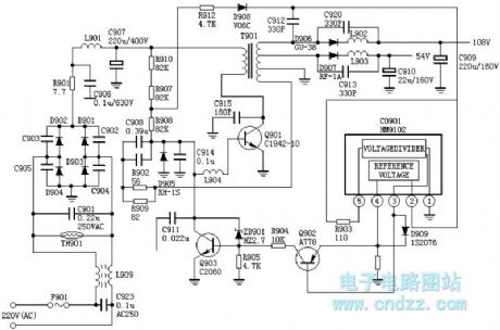
The models using Hitachi NP8C power supply are: Hitachi CTP236, CEP320D, CRP350D, 450D, Furistock HFC-236, 450, Goldstar C37-401, C46-1, C563, etc. This power supply is widely used for early period color TV in China.
Oscillating process
300V DC voltage is added to switching tube Q901's B pole through R911, R907 and R908. Q901 starts to break over. T901's primary winding has current, at the same time, it can generate induction voltage, its polarity is that up is positive and down is negative. So this stage winding also can generate induction voltage, the polarity is thatdown is positive and up is negative. This voltage is sending to Q901's B pole through R902, R909 and C908, and it can make Q9021 break over further, the strong positive feedback makes Q901 rapidly saturation. (View)
View full Circuit Diagram | Comments | Reading(3127)
Practical circuit of full bridge switching stabilized voltage supply
Published:2011/11/14 2:37:00 Author:May | Keyword: full bridge, switching, stabilized voltage supply

The diagram is practical circuit of full bridge switching stabilized voltage supply. It is 1500W double pole power switching stabilized voltage supply circuit controlled by CW194. In the circuit, four double pole high back voltage transistors F661 are switching tube. Controlled by integrated circuit CW494, two pairs tubes are breaking over and cutting off in turns. It can change DC to high frequency AC. Then the high frequency AC is passing high frequency transformer to step-down. After rectifying and filtering, it will get 12V DC stabilized voltage. F661 power switching tube's BVceo≥400V. Time of toff is 1μs. So in the conditionwith high power, its power consumption is small.
The core component of this circuit is high-frequency transformer. Its magnetism performance has high requirement: frequency characteristic requires to reach megahertz; saturation magnetic flux density must reach to 5000Gs; magnetic hysteresis loss must be small; when it uses EC70 magnetic core, output power is 1000W; when it uses EC90 magnetic core, output power is 2000W. (View)
View full Circuit Diagram | Comments | Reading(1520)
Full bridge power inversion circuit
Published:2011/11/14 2:35:00 Author:May | Keyword: Full bridge, power inversion
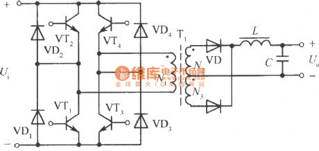
Full bridge inversion circuit is shown in the diagram and consists of suitable driver circuit and half bridge converter which hastwo electrolytic capacitors. Four bridge arms consist of VT1, VT2, VT3 and VT4. High frequency transformer T is connected in the middle of them. VT1, VT4 and VT2, VT3 on opposite arms is breaking over in turns by excitation of drive circuit. They can change DC input voltage to high frequency square wave AC voltage. Its working process is the same as push pull power converting circuit. So when high frequency transformer is working, the voltage gotten by its primary coil is power supply voltage. It is one time of half bridge circuit's output voltage, but each transistor's withstand voltage is still power supply voltage, so the output voltage is enlarging one time. If you want to let the current reach the level of half bridge circuit, the current shoule be enlarged one time, the output power can beenlarged four times.
The main shortcoming of full bridge circuit is that it needs four groups transistors base drive circuit which are isolatingfrom each other, so the control drive circuit is complex and expensive. (View)
View full Circuit Diagram | Comments | Reading(1076)
Jinxin TDA two chip system power supply
Published:2011/11/14 3:31:00 Author:May | Keyword: Jinxin TDA, two chip system, power supply

This power supply is also known as X53P power supply or X56P power supply. Taking Jinxing C498 for example, we simply introduced the principle of working.
Oscillating process
About 300V DC voltage on C708 adds to B pole of switching tube V720 by R729, R731 and L711. V720 starts to turn on. C pole's current is enlarging. T705's pin 1 and 12 generate induced electromotive force. Its polarity is that 1 is positive and 12 is negative. The positive feedback winding also generates negative induced voltage. Its polarity is 10 is positive and 9 is negative. This feedback voltage is added to B pole of V720 by C713, V713 and R713. It can make V720's current increase. Looping like this can make V720 saturation rapidly.
Voltage regulation process
Voltage regulation circuit consists of V745 and peripheral components. The sampling winding is T705's 7 and 8 winding. The voltage passes through V741 rectifying and C745 filtering. The voltage on C745 reflects the size of output voltage. If output voltage is increasing, the voltage on C745 is increasing too. (View)
View full Circuit Diagram | Comments | Reading(931)
Switching power supply type high voltage constant current source circuit diagram
Published:2011/11/14 1:58:00 Author:May | Keyword: Switching power supply, high voltage, constant current source

To develop a device instrument, we need a constant current source which can generate 1MA current on the resistor with the resistance value of0~3MΩ. We designed one by using UC3845 and 12V storage battery. Transformer adopts color TV high voltage package. L1 uses enameled wire to go around 24 turns on original high voltage package magnetic core. L3 gets help from one turn of original high voltage package. L2 gets help from high-voltage parts of high voltage package. Voltage limiting circuit consists of L3 and LM393. It can limit the output voltage and make it not too high. It can adjust the voltage of open circuit by adjusting R10. (View)
View full Circuit Diagram | Comments | Reading(6993)
Kaige 4C7108 power supply
Published:2011/11/14 2:03:00 Author:May | Keyword: Kaige, power supply

Kaige 4C7108 adopts separated exciting single-end fly-back converter type switching power supply. Oscillating circuit adopts TDA83820. Main power supply output voltage is 115V.
Voltage regulator circuit
Voltage regulator circuit mainly consists of components of Q503, Q504, IC502, etc. Difference amplifier composed of Q503 and Q504, whichare error sampling circuit. D519 offers reference voltage for Q503. B pole of Q504 changes along with output voltage. When output voltage is too high, the break over level of Q504 is decrease, and Q503's C pole current is dividing, then it will decreasing. The current of IC502 is increasing. Internal resistance of IC502's pin 4, 5 is decreasing. The voltage of IC501's pin 9 is decreasing. The duty factor of widened pulse is decreasing. Then output voltage is decreasing. So it reaches the purpose of voltage regulation. It can change output voltage by adjusting VR504. (View)
View full Circuit Diagram | Comments | Reading(1718)
Controlled silicon switching stabilized voltage supply
Published:2011/11/14 2:30:00 Author:May | Keyword: Controlled silicon, switching stabilized voltage supply

When controlled silicon switching stabilized voltage supply is normal working, it uses very small control currentto control very high anode current.
The diagram showsa practical circuit of controlled silicon ripples trigger type switching stabilized voltage supply. It shapes and enlarges of rectified ripple. Then it can trigger controlled silicon and make it break over. When the momentary value of rectified voltage is dropping to 0V, controlled silicon will becut off byitself. It can achieve voltage regulation by using the changes of output voltage to control the leading edge of trigger pulse.
Voltage regulator circuit mainly consists of transistors VT1~VT4, transformer T, controlled silicon SCR1, etc.
When the power supply turns on, rectifier can output pulse DC voltage like wave ①. It adds to the base of VT4 after diving by R2 and R3, the wave is shown in ②. VT4 can enlarge it, then collector output pulse can charge to C7 through R8, so it can generate run up saw-tooth wave. The wave is sent to the base of VT3 through R7, its wave is shown in ③. (View)
View full Circuit Diagram | Comments | Reading(935)
The clamping single-end normal shock converter circuit with two transistors and diode
Published:2011/11/14 2:32:00 Author:May | Keyword: Two transistors , diode, clamping, single end, normal shock converter
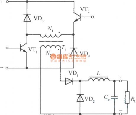
The following diagram is the clamping single-end normal shock converter circuit with two transistors and diode. VT1 and VT2are energized by PWM pulse and broken over and cut off at the same time. When they are cut off, polarity on N1 is reversing, diodes VD3 and VD4 are broken over, the potential is clamped. So, when VT1, VT2 are cut off, the voltage amplitude added between collectors are equal to input voltage Ui. (View)
View full Circuit Diagram | Comments | Reading(1116)
| Pages:380/2234 At 20361362363364365366367368369370371372373374375376377378379380Under 20 |
Circuit Categories
power supply circuit
Amplifier Circuit
Basic Circuit
LED and Light Circuit
Sensor Circuit
Signal Processing
Electrical Equipment Circuit
Control Circuit
Remote Control Circuit
A/D-D/A Converter Circuit
Audio Circuit
Measuring and Test Circuit
Communication Circuit
Computer-Related Circuit
555 Circuit
Automotive Circuit
Repairing Circuit