
Circuit Diagram
Index 370
Resistor - transistor gate circuit
Published:2012/8/11 1:48:00 Author:Ecco | Keyword: Resistor - transistor gate

Figure (a) is theresistor - transistor gate circuit diagram , it is similar to the ordinary NAND gate, but each input endisconnectedto a Rk with the samevalue.
Figure (b) shows its logic symbol .
(View)
View full Circuit Diagram | Comments | Reading(984)
Comparator circuit with hysteresis characteristics (Schmitt trigger )
Published:2012/8/11 1:39:00 Author:Ecco | Keyword: Comparator , hysteresis characteristics , Schmitt trigger
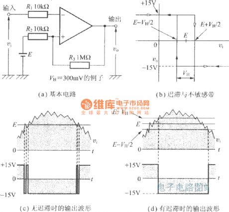
(a)The basic circuit; (b)Hysteresis and non- sensitive zone; (c)The output wave without hysteresis; (d)The output wave with hysteresis
(View)
View full Circuit Diagram | Comments | Reading(1701)
Three-terminal integrated voltage regulator constant current source circuit
Published:2012/8/12 21:00:00 Author:Ecco | Keyword: Three-terminal , integrated , voltage regulator , constant current source

Figure 1 shows the constant current source circuit composed of 7805. Resistor R is connected at the output and public ends to form a fixed constant current, then thecurrent flows through the load RL and then back to power supply. Regulator works in the suspended state. The circuit uses regulator to change its own differential pressure to maintain constant current flowing through the load when the load changes. Output current Io = 5V / R 10 ID,in the formula, ID = 1.5mA ( using 7805 , ID = 1.5mA ). Therefore, changing the size of the R can adjust output current.
(View)
View full Circuit Diagram | Comments | Reading(1951)
The level shift circuit diagram completed by PNP transistors
Published:2012/8/12 21:40:00 Author:Ecco | Keyword: level shift, PNP transistor

PNP transistor forms common-emitter amplifier circuit to ensure that the transistors work in the enlarged area, and the collector level must be less than the base level. So, in the NPN multi-stage DC amplifier circuit, inserting a PNP transistor common-emitter amplifier circuit can complete the displacement of DC level and zoom function. (View)
View full Circuit Diagram | Comments | Reading(5354)
The level shift circuit diagram completed by constant flow source
Published:2012/8/12 21:54:00 Author:Ecco | Keyword: level shift , constant flow source
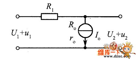
The DC internal resistor Ro of constant current source is very small, AC internal resistor ro is great, when the R1 》 Ro and R1 《 ro, the DC level U2 of output end is much lower than DC level U1 of the input end, namely U2 《 U1. AC voltage u2 of output end decreases little from input AC voltage u1, that is, u2 ≈ u1. Therefore, the circuit decreases DC level under the circumstance without losing AC voltage.
(View)
View full Circuit Diagram | Comments | Reading(719)
Practical circuit diagram to expand current with external PNP power transistor
Published:2012/8/12 21:59:00 Author:Ecco | Keyword: Practical circuit , expand current, external , PNP , power transistor
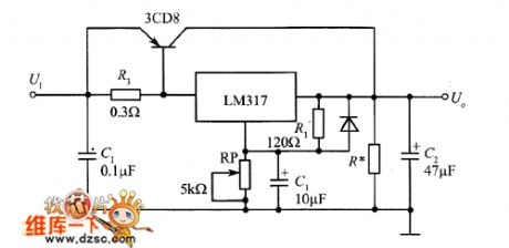
Expanding output current can be realized in two ways: connecting external high-power tubes; connected two or more integrated voltage regulators in parallel. The figure shows practical circuit using an external PNP power transistor to expand the output current, and the method is simple but reduces the precision of the regulator.
(View)
View full Circuit Diagram | Comments | Reading(1517)
The fixed low - voltage output circuit diagram of three-terminal adjustable output regulator
Published:2012/8/12 21:16:00 Author:Ecco | Keyword: fixed, low - voltage output , three-terminal , adjustable output, regulator
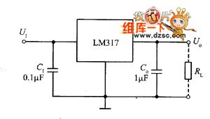
The figure shows the resistor network without adjustable outpu , and it gets 1.25V fixed low-voltage output circuit. The temperature drift is low, which is only decided by the temperature drift of internal reference voltage source.
(View)
View full Circuit Diagram | Comments | Reading(616)
3.6W mobile phone battery charger circuit diagram
Published:2012/8/12 20:47:00 Author:Ecco | Keyword: 3.6W , mobile phone , battery charger

The3.6W charger circuit special for mobile phone is shown as the figure, andthe power supplyhas constant current / constant voltage output characteristics, and the no-load power consumption is less than 100mW. It can provide constant current charging for nickel-metal hydride (NiMH) batteries or nickel cadmium (NiCd) batteries, lithium ion ( Li = ion) batteries inmobile phone. Its main technical index: AC input voltage u = 85 ~~ 265V, output voltage Uo = 5.2V , the maximum output current Iom = 0.697A, output power Po, = 3.6W.
(View)
View full Circuit Diagram | Comments | Reading(4793)
Transistor performance quick test circuit
Published:2012/8/12 21:29:00 Author:Ecco | Keyword: Transistor , performance, quick test

The figure transistor performance quick test circuit. In the figure, HFC9300is music IC which stores a song. BL is a speaker , S is the trigger switch . VTx is a transistor undertest. When VTx inserts into the socket, and thepin collectorinsertsinto c , the base inserts into b , the emitter inserts into e . If VTx is a good tube, BL will play a beautiful song; if VTx is a bad tube , then BL keeps silence.
(View)
View full Circuit Diagram | Comments | Reading(1197)
The caple amplifier circuit composed of OPA660
Published:2012/8/12 22:10:00 Author:Ecco | Keyword: caple amplifier

Cable input signal VI is added to the pin 3 of OPA660 after passing 150Ω base resistor and 50Ω matched resistor, then it is output by pin 6 after being amplified by the internal OTA and +1 amplifier ( resistor RQ is not shown in figure in quiescent current ). Circuit gain G = RL / (RE + rE ) = +3.
(View)
View full Circuit Diagram | Comments | Reading(986)
Fundamental Pierce oscillator circuit
Published:2012/8/12 22:29:00 Author:Ecco | Keyword: Fundamental Pierce , oscillator

The oscillator uses a fundamental quartz crystal, and the oscillation frequency can be up to 10MHz. Oscillator circuit is tuned to the resonant frequency. Capacitor C requires below 4.7pF, and it is connected to a follower to isolate the quartz crystal circuit.
(View)
View full Circuit Diagram | Comments | Reading(2070)
The quartz crystal oscillator circuit using NAND gate
Published:2012/8/12 22:31:00 Author:Ecco | Keyword: quartz crystal oscillator , NAND gate

The circuit uses two 7400 TTL NAND gates, the oscillator frequency can reach 18MHz. Two 820 Ω resistors must be selected by oscillator frequency.
(View)
View full Circuit Diagram | Comments | Reading(2069)
The OPA606 broadband Difet operational amplifier circuit
Published:2012/8/11 1:43:00 Author:Ecco | Keyword: broadband , Difet, operational amplifier


Simplified schematic:
The zeroing cable diagram:
noninverting amplifier:
inverting amplifier:
Buffer wiring diagram:
(View)
View full Circuit Diagram | Comments | Reading(1083)
Y-connection motor protection circuit
Published:2012/8/11 1:35:00 Author:Ecco | Keyword: Y-connection , motor , protection

In the circuit shown as the figure, pressing the ST will make KM coil get electric and pull in; loosening ST will allow the KM to get self-protection, then motor M runs. When one phase of three-phase alternating current circuit is dieconnected, then motor's midpoint will generate potential difference. The voltage will be rectified and stabilized to make relay K be energized, then the power of M is cut to to protect the motor stator windings from burning. The circuit is suitable for motors with power lowering than 7.5kW.
(View)
View full Circuit Diagram | Comments | Reading(1937)
M1040 centerless grinding machine circuit
Published:2012/8/11 1:12:00 Author:Ecco | Keyword: centerless grinding machine
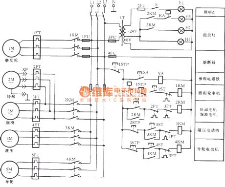
The centerless grinding machine is composed of grinding wheel, guide wheel , cooling, lubrication and hydraulic motor, and the circuit is shown in the figure. Before launching the grinding wheel motor 1M, the lubrication pump motor 3M should be started firstly to make the spindle dynamic bearing of grinding wheel fill with lubricating oil, then the oil returning make the floats rise, then the flowing relay KA's contacts are connected in order to start grinding wheel motor 1M. If the oil disappears, the device will be automatically stopped.
(View)
View full Circuit Diagram | Comments | Reading(3377)
Three-way blinking light string circuit (1)
Published:2012/8/6 4:20:00 Author:Ecco | Keyword: Three-way , blinking, light string
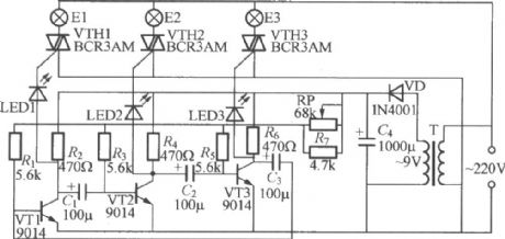
The figure shows a three-way flashing light string controller which is simple and easy to make, and each way can drive power up to 600W. Ifthree-way light strings are arranged appropriately in space, it can form light liquidity effect visually.
(View)
View full Circuit Diagram | Comments | Reading(1359)
Thermal pyroelectric infrared sensing automatic light circuit (6)
Published:2012/8/6 4:14:00 Author:Ecco | Keyword: Thermal, pyroelectric , infrared , sensing , automatic light
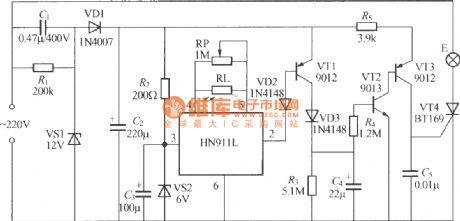
As shown in the figure, it isa sensing automatically lightmade by newHN911L pyroelectric infrared detection module. The HN911L integrates high - sensitivity infrared sensors, PIR , amplifiers, signal processing circuit andoutput circuit. Itisable to remote sense the faint infrared signals from human motion. The lights can be turned on when people move around, turned off automaticallydelay tens of seconds when people leave.
(View)
View full Circuit Diagram | Comments | Reading(2734)
Current-comparator NORTON four op amp MC3301/3401
Published:2012/8/6 4:29:00 Author:Ecco | Keyword: Current-comparator, NORTON, four op amp

Figure (a)is simplifiedschematic diagram; Figure(b)is the inverting input amplifier circuit; Figure (c)is the noninverting input amplifier circuit.
(View)
View full Circuit Diagram | Comments | Reading(1401)
The basic op amp circuit for voltage stabilization
Published:2012/8/6 4:35:00 Author:Ecco | Keyword: basic op amp , voltage stabilization

In the circuir, the value of R1~R3 can be selected by the required regulated value. UA is higher than UZ. The voltageof circuit shown in the figure b can be regulated by RP. The regulating range of voltage UA is about 2V~(UB-2V).
(View)
View full Circuit Diagram | Comments | Reading(1042)
The water height alarm circuit diagram
Published:2012/8/6 4:23:00 Author:Ecco | Keyword: water height , alarm
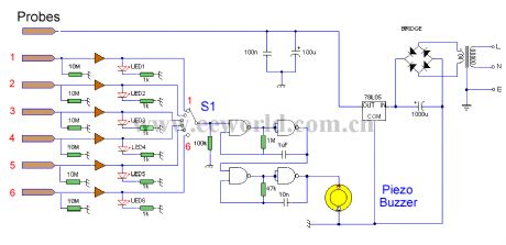
This circuit will trigger with any fluid with a resistance under 900K between the maximum separation distance of the probes. Let me explain further. The circuit uses a 4050B CMOS hex buffer working on a 5 volt supply. All gates are biased off by the 10M resistors connected between ground and buffer input. The common probe the topmost probe above probe 1 in the diagram above is connected to the positive 5 volt supply. If probe 1 is spaced 1 cm away from the common probe and tap water at 25 ?C is detected between the probes (a resistance of 20k) then the top gate is activated and the LED 1 will light. Similarly if probe 2 at 2 cm distance from the common probe detects water, LED 2 will light and so on. Switch 1 is used to select which output from the hex buffer will trigger the audible oscillator made from the gates of a CMOS 4011B IC.Placement of Probes:As 7 wires are needed for the probe I reccommend the use of 8 way computer ribbon cable. The first two wires may be doubled and act as the common probe wire. Each subsequent wire may be cut to required length, if required a couple of millimetres of insulation may be stripped back, though the open cut off wire end should be sufficient to act as the probe. The fluid and distance between probe 6 and the common probe wire must be less than 900k. This is because any voltage below 0.5 Volt is detected by the CMOS IC as logic 0. A quick potential check using a 900k resistance and the divider formed with the 10M resistor at the input proves this point: 5 x (0.9 / (0.9+10) = 0.41 Volt. (View)
View full Circuit Diagram | Comments | Reading(1716)
| Pages:370/2234 At 20361362363364365366367368369370371372373374375376377378379380Under 20 |
Circuit Categories
power supply circuit
Amplifier Circuit
Basic Circuit
LED and Light Circuit
Sensor Circuit
Signal Processing
Electrical Equipment Circuit
Control Circuit
Remote Control Circuit
A/D-D/A Converter Circuit
Audio Circuit
Measuring and Test Circuit
Communication Circuit
Computer-Related Circuit
555 Circuit
Automotive Circuit
Repairing Circuit