
Circuit Diagram
Index 363
MRFICl505R2 - based GPS receiver RF front-end circuit
Published:2012/8/25 0:56:00 Author:Ecco | Keyword: GPS receiver , RF, front-end

MRFICl505R2 is a 1.575GHz GPS downconverter chip. It integrates mixer, VCO, PLL, crystal oscillator, A / D converter and loop filter and other circuits. MRFICl505R2 IF output frequency is 4.1MHz; it has 105dB typical conversion gain, 2.7V operating voltage, 28mA typical current consumption; it is available in LQFP-48 package.
(View)
View full Circuit Diagram | Comments | Reading(1739)
Ordinary thyristor measured by battery
Published:2012/8/23 22:51:00 Author:Ecco | Keyword: Ordinary thyristor , battery

It takes four 1.5V batteries connected in series, then switch S is connected, E1 cathode is connected to anode of ordinary thyristor VS by lamp HL. E2 negative pole is connected to VT cathode. Close the S, HL is not extinguished. Because the lamp resistance is small, the current flowing through VT is sufficient to maintain triggered conduction current. Only disconnecting the anode or cathode connection of the thyristor, VT will shutdown, HL is extinguished.
(View)
View full Circuit Diagram | Comments | Reading(1204)
Two regulators connecting in series to get 0 ~ 284V voltage
Published:2012/8/23 22:46:00 Author:Ecco | Keyword: Two regulators, connecting, in series, 0 ~ 284V voltage
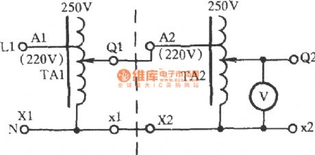
As shown in the figure, the two regulators TAl and TA2 are connected in series to obtain 0 ~ 284V voltage. The two regulators' X1, X2 are connected with a wire together, then the power zero line N is connected;220V power supply is connected between Al andX1. The output terminal Q1 of TA1 is connected to A2 end of TA2. After energized,it can get 0 ~ 284V voltage betweenTA2 outputend andQ2, and voltage regulator issmooth.
(View)
View full Circuit Diagram | Comments | Reading(641)
Three regulators with star connection to get 0 ~ 433V voltage
Published:2012/8/23 22:40:00 Author:Ecco | Keyword: Three regulators , star connection , 0 ~ 433V voltage
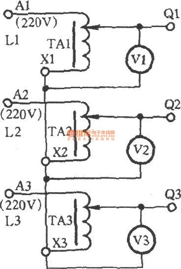
As shown in the figure, three regulators TA1 , TA2, TA3 are connectedas star connection to expand pressure range and get the maximum attainable 433V voltage . The three regulators' X1, X2, X3 ends areconnected together, A1 , A2 , A3 are respectively connected to the 380V power's L1, L2, L3 three phases, so itobtains 433V at the output terminals Q1 and Q2 or Q2 or Q3 ends. This connection requires a three-phase voltage balance, TA1, TA2 and TA3 models and specifications must be the same.
(View)
View full Circuit Diagram | Comments | Reading(751)
Leakage Ground Fault point measuring by Clamp meter
Published:2012/8/23 22:36:00 Author:Ecco | Keyword: Leakage , Ground Fault point, Clamp meter

When the distribution lines or motor control equipment occursleakage Ground Fault, it is more difficult to identify the specific ground fault point. But Clamp ammeter canmeasure leakage ground fault without power outage andwiring,the circuit isshown as the figure.
(View)
View full Circuit Diagram | Comments | Reading(1723)
The analog USB with homemade USB port ISP2313
Published:2012/8/23 22:54:00 Author:Ecco | Keyword: analog USB , homemade, USB port


Many laptops have no serial or parallel port. In this case, people only can use the USB port ISP. The production is not using a real USB chip, but with 2313 to copy USB timing.
(View)
View full Circuit Diagram | Comments | Reading(1095)
The interface circuit of sampling and maintaining amplifier AD9101
Published:2012/8/23 22:11:00 Author:Ecco | Keyword: interface circuit , sampling, maintaining, amplifier

When the signal frequency increases, the traditional fast sampling circuit is forced to sacrifice dynamic range for the stability of the overall performance. The circuit shown in figure uses AD9101 to match with high - speed 8 - bit A / D converter AD9002, the purpose is to enhance the high frequency performance of the Flash ADC; simultaneously with the regulator and output of op-amp voltage follower, the circuit increases AD9101 RTN feet potential to 0 .33 V.
(View)
View full Circuit Diagram | Comments | Reading(571)
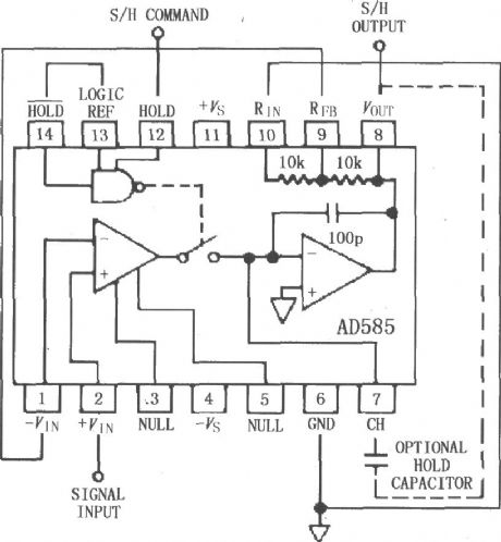
AD585 high-speed precision sampling and maintaining amplifier
Published:2012/8/23 22:15:00 Author:Ecco | Keyword: high-speed, precision , sampling , maintaining, amplifier

The AD585 is a complete monolithicsampling and maintaining amplifier, including a high-performance operational amplifier series with a very low leakage current switch and a FET input integrated amplifier. The internal holding capacitor and matching applications resistors provide precision and flexibility. The AD585's quick sampling time, low sample-and-hold disorders and fall characteristics make it ideal for high-speed 10 ~ 12bit data acquisition system. The pin configuration is shown as the figure.
(View)
View full Circuit Diagram | Comments | Reading(785)
The AD585 HOLD effective sample - hold circuit with gain = +2
Published:2012/8/23 22:16:00 Author:Ecco | Keyword: HOLD, effective , sample - hold , gain = +2
View full Circuit Diagram | Comments | Reading(1251)
Tracking - hold intermediate frequency (IF) signal acquisition circuit (AD9100/AD9618)
Published:2012/8/23 22:21:00 Author:Ecco | Keyword: Tracking - hold , intermediate frequency , signal acquisition
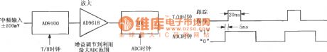
AD9100 has a wide dynamic range, and therefore can be used to capture the super signal, and it can directly convert the intermediate frequency signal (IF) to digital signal. After IF signal is input AD9100, T / H clock control sampling and holding, then the signal is output and amplified by AD9618, and the ADC circuit converts the analog signal to a digital signal. With reducing analog signal input level, the method can realize the track and hold with a minimum distortion; while adjusting the AD9618 gain, the analog signal range input to ADC meets the full scale range of the A / D converter - digital conversion.
(View)
View full Circuit Diagram | Comments | Reading(598)
A part of product detector circuit composed of LF198 and LM122H
Published:2012/8/23 22:27:00 Author:Ecco | Keyword: product detector

Synchronous clock signal is input to a cascade of timer circuit composed of two LM122H, then the synchronization clock is converted to the desired width of the pulse (Fig. 10μs) which will be add to LF198 LOGIC end (8 feet) as the sampling and holding control signal . The signal is input LF198's pin 3. The input signal contains a large number of noise component with magnitude higher than the useful signal, after the detector, the output signal's noise is filtered off, a pure signal will be output. The value of R3 should make 6-pin voltage be 0 ~~ 3V.
(View)
View full Circuit Diagram | Comments | Reading(2086)
Time incremental sampling differential measurement circuit composed of SMP04 and instrumentation amplifier
Published:2012/8/23 20:58:00 Author:Ecco | Keyword: Time incremental, sampling , differential , measurement circuit, instrumentation amplifier

The circuit is used for measuring the difference of signal voltage at the different time points, that is the difference between voltages V1 and V2 at t1 and t2. Because the circuit uses the sampling and maintaining amplifier with the same package of SMP04, the symmetry of the circuit is good. The signal is output by SMP04, then it is sent to the instrument amplifier AMP02 for differential amplification, RG is used to set the instrument amplifier gain. VOUT = G (V1-V2), G = 50k/RG +1.
(View)
View full Circuit Diagram | Comments | Reading(1231)
Precision current inverter / current source circuit 1 composed of LOG101/104 and op amp OPA2335
Published:2012/8/23 21:36:00 Author:Ecco | Keyword: Precision , current inverter, current source , op amp
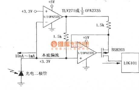
LOG101/104 's input current can only be positive current, that is, input current only flows into pin 1 and pin 8, which can be fine tuned as 10nA to 1mA. In some applications, the signal current is a negative current, such as: photomultiplier, tube, photodiode. The circuit shown in diagram can resolve this problem, which utilizes the circuit switch the negative signal current generated by photodiodes to a forward current flowing into LOG101.
(View)
View full Circuit Diagram | Comments | Reading(1404)
Precision current inverter / current source circuit 2 composed of LOG101/104 and op amp OPA2335
Published:2012/8/23 21:39:00 Author:Ecco | Keyword: Precision, current inverter , current source circuit , op amp
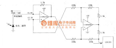
The negative signal current generated by the photodiodecan be converted to the forward current flowing into LOG101 by two op amps OPA2335.
(View)
View full Circuit Diagram | Comments | Reading(917)
Current allocation multiplexing circuit composed of double broadband transconductance operational amplifier OPA2662
Published:2012/8/23 21:57:00 Author:Ecco | Keyword: Current allocation , multiplexing, double broadband , transconductance, operational amplifier
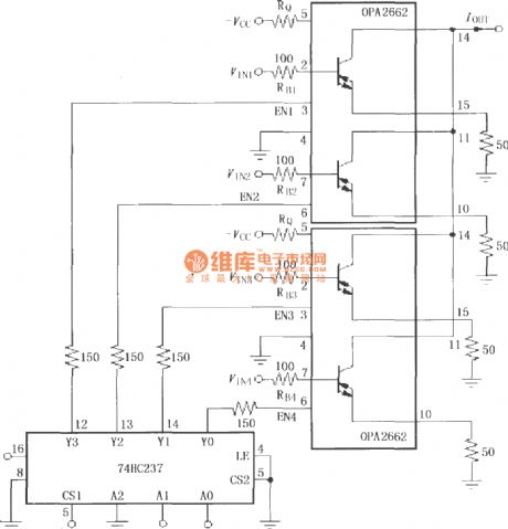
74HC237 is the address latch 3 line - to - 8 line decoder, three-way encoded signals A1, A2, A3 are input 74HC237 to decode and output decoded signals Y0 , Y1 , Y2, and Y3, and they can respectively control two OPA2662 and enable terminal EN to output different paths of current, then the current allocation multiplexing circuit is made up.
(View)
View full Circuit Diagram | Comments | Reading(1070)
Two-channel current output driver circuit composed of double broadband transconductance operational amplifier OPA2662
Published:2012/8/23 22:05:00 Author:Ecco | Keyword: Two-channel , current output , driver circuit , double broadband , transconductance, operational amplifier
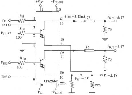
The circuit uses OPA2662 internal dual OTA to constitute two-channel current output driver circuit, and input signals VIN1 and VIN2 are amplified by OPA2662 to output current IOUT1 and IOUT2 for driving current to drive 75Ω cable and load. EN1, EN2 can control turning on or off of channels, when EN is in high level, the channel is turned on; when EN is in low level, the channel is turned off.
(View)
View full Circuit Diagram | Comments | Reading(1032)
The basic signal and power connection circuit of broadband transconductance operational amplifier and buffer OPA660
Published:2012/8/22 21:38:00 Author:Ecco | Keyword: basic , signal , power, connection , broadband , transconductance, operational amplifier , buffer

It is the connection circuit for op amp OPA660, the signal is input by pin 3, then pin 8 will output current after the signal being amplified. Power supply terminal uses bypass capacitor filter which preferably uses solid tantalum capacitor as a filter capacitor, and the design of the PCB should allow the filter capacitor to close to the power supply terminal. Quiescent current is set by external resistor RQ connected to pin 1 and -VCc, and the change of resistor RQ can affect internal OTA of OPA660 to control their bandwidth, AC performance and transconductance. When ambient temperature at 25 ℃, OPA660 provides typically 20mA total quiescent current IQ, and that can be eached by setting RQ = 250Ω. The quiescent current IQ can change in the range of 16 ~ 26mA when RQ is fixed as 250Ω.
(View)
View full Circuit Diagram | Comments | Reading(1252)
Logic control prohibit circuit composed of broadband transconductance op amp and buffer OPA660
Published:2012/8/22 22:11:00 Author:Ecco | Keyword: Logic control , prohibit circuit , broadband transconductance, op amp, buffer

The circuit adds a transistor 2N2907 to control pin 1 of OPA660 1. When the 2N2907 base is extremely 0V, transistor gets conduction, Ic = 1mA, RQ voltage rises to 1V which is higher than the negative power supply (-5V), OPA660's static current is reduced to 0, OPA660 is prohibited from working; Conversely, when the base is extremely 5V, the transistor is cut, Ic = 0mA, RQ voltage drops to make OPA660 quiescent current increase, OPA660 is allowed to work.
(View)
View full Circuit Diagram | Comments | Reading(997)
The antilogarithm circuit composed of logarithmic and logarithmic ratio amplifier LOG100
Published:2012/8/22 21:47:00 Author:Ecco | Keyword: antilogarithm , logarithmic , logarithmic ratio , amplifier
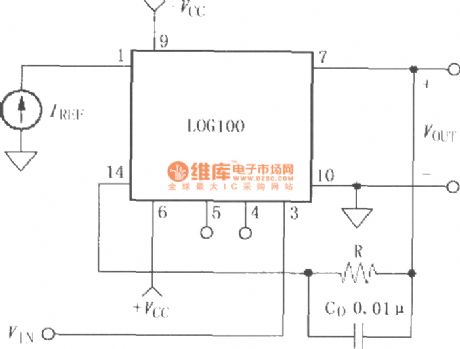
The circuit transformslogarithmic amplifier LOG100into antilog circuit. When VIN connects to pin 3, k=1; when VIN connects to pin 4, K =3; when VIN connects to pin 5, K =5.
(View)
View full Circuit Diagram | Comments | Reading(698)
Video luminance matrix circuit composed of broadband transconductance op amp and buffer OPA660
Published:2012/8/22 21:59:00 Author:Ecco | Keyword: Video, luminance matrix , broadband transconductance, op amp , buffer
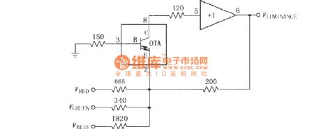
The OPA660 forms a common-base amplifier circuit, and its pin 2 has three-way signal inputs: red VRED, green VGREEN and blue VBLUE, the signals are amplified by internal OTA and +1 amplifier to become luminance signal VLUMINANCE which is output from pin 6. The accuracy of the resistor connected to three-way signals is 1 %, resulting in the RGB mixing ratio of 30%: 59%: 11%.
(View)
View full Circuit Diagram | Comments | Reading(1241)
| Pages:363/2234 At 20361362363364365366367368369370371372373374375376377378379380Under 20 |
Circuit Categories
power supply circuit
Amplifier Circuit
Basic Circuit
LED and Light Circuit
Sensor Circuit
Signal Processing
Electrical Equipment Circuit
Control Circuit
Remote Control Circuit
A/D-D/A Converter Circuit
Audio Circuit
Measuring and Test Circuit
Communication Circuit
Computer-Related Circuit
555 Circuit
Automotive Circuit
Repairing Circuit