
Circuit Diagram
Index 367
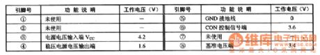
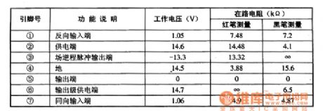
Typical application circuit of two- wire smart Hall sensor IC TLE4941
Published:2012/8/16 0:59:00 Author:Ecco | Keyword: Typical application , two- wire, smart, Hall, sensor IC
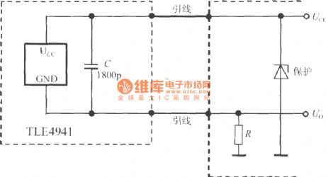
C is the de-noising capacitor. Output currentcan be converted into voltage signal Uo byresistor Rand sent todigital voltmeter (DVM), or microcontroller with ADC.
(View)
View full Circuit Diagram | Comments | Reading(1153)
TDA7274 motor speed stabilizing control integrated circuit diagram
Published:2012/8/16 23:01:00 Author:Ecco | Keyword: motor, speed stabilizing, control, integrated circuit
The TDA7274 is the motor speed stabilizing control integrated circuit produced by a European company, and it is widely used in music players, video machines and electronic toys.(1) Features and functionsTDA7274 IC internal circuit contains reference power supply circuit, error amplification circuit, motor speed control circuit and a number of other subsidiary circuits.(2) Pin functions and dataThe TDA7274 IC uses 8-pin dual in-line package, and the pin functions and data are shown in Table 1.Tip : TDA7274 IC and the domestic model SG7274 can be interchangeable.
(View)
View full Circuit Diagram | Comments | Reading(944)
TDA8177 field scanning output IC diagram
Published:2012/8/16 21:57:00 Author:Ecco | Keyword: field , scanning , output , IC
The TDA8177 is the field scanning output IC produced by French Thomson, which is widely used in a variety of rear-projection color TV at home and abroad, such as the HP clear fine rear projection color TV.
(1) Features and functionsTDA8177 IC 's operating supply voltage range is wider, and the highest supply voltage can be up to 35V, output current can be up to 3A, flyback voltage can be up to 70V. TDA8177 integrated circuit contains the scanning power amplifier, flyback pulse generating circuit, overheating protection and over-current protection circuit, and it is suitable for DC coupling working way.
2 pin functions and dataThe TDA8177 IC uses a separate 7-pin package, and pin functions and data are listed in Table 1.
(View)
View full Circuit Diagram | Comments | Reading(1260)
Analog capacitance meter ( CD4013 )
Published:2012/8/17 1:43:00 Author:Ecco | Keyword: Analog capacitance meter

With a dual D flip-flop CD4013, a trigger and the measured capacitor form a monostable multivibrator toproduce the output pulse, the output pulse width,current average value and of the capacitance of the measuredcapacitor areproportional. The other flip-flop can form a multivibrator to generate the trigger pulse. An IC can form a simple capacitance meter. The measuring range : l00pF ~ lμF.
(View)
View full Circuit Diagram | Comments | Reading(5154)
Thermostat schematic of thermistor electric water heater
Published:2012/8/16 22:27:00 Author:Ecco | Keyword: Thermostat schematic , thermistor, electric water heater

The circuit consistes of thermistor RT, comparator, driverand heater RL. The circuit can keep water temperature at 90 ℃ by automatically opening and closing control of the heater.
When temperature is at 25 ℃ thermistor resistance is 1OOkΩ, temperature coefficient of 1K / ℃. When comparator's inverting input end is added the 3.9V reference voltage, the comparator's noninverting input terminal is added the partial pressure voltage of RP and thermistor RT. When the water temperature belows 90 ℃, the comparator IC outputs high potential to drive VT1 and VT2 conduction, then the relay K works, heater circuit is closed; when the temperature is higher than 90 ℃, comparator IC output is in low potential, VT1 and VT2 are cut-off, the heater circuit is disconnected by relay K. Adjusting RP obtain the required water temperature.
(View)
View full Circuit Diagram | Comments | Reading(3943)
The counter circuit composed of HK-1 Hall approach switch
Published:2012/8/15 23:10:00 Author:Ecco | Keyword: counter circuit , Hall , approach switch
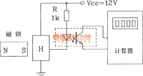
The circuit shown in figure uses optocoupler isolatior and 8 -bit calculator. Whenever the magnet closes to the HK-1 switch once, the calculatorcounts a number and accumulates, thus completing the count function.
(View)
View full Circuit Diagram | Comments | Reading(630)
Acousto-optic detector circuit to measure the crystal
Published:2012/8/15 22:30:00 Author:Ecco | Keyword: Acousto-optic , detector , measure , crystal

The circuit is shown in Figure, which consists of capacitance three-point oscillator, isolation level, voltage doubler rectifier circuit and stereo sound circuit and flash display circuit. It can detect the crystal's goodness or badness, good crystal will issue the sound of Didi ... , and LED1, LED2 will be blinking; bad crystal will not issue audible and visual information.
(View)
View full Circuit Diagram | Comments | Reading(1331)
Analog frequency meter circuit
Published:2012/8/15 22:10:00 Author:Ecco | Keyword: Analog , frequency meter

The circuit can measure the frequency between 1.5kHz ~ 500kHz by connecting C1 ~ C6 different capacitors. The maximum frequency is up to 1MHz. Transistor T1 can be used as the integrator, and its load resistor is 15kΩ resistor and R1 ~~ R6 adjustable resistors. Integrator's input signal is about 4 to 10V ( peak - peak value).
(View)
View full Circuit Diagram | Comments | Reading(3159)
Binary counter circuit
Published:2012/8/15 23:05:00 Author:Ecco | Keyword: Binary counter
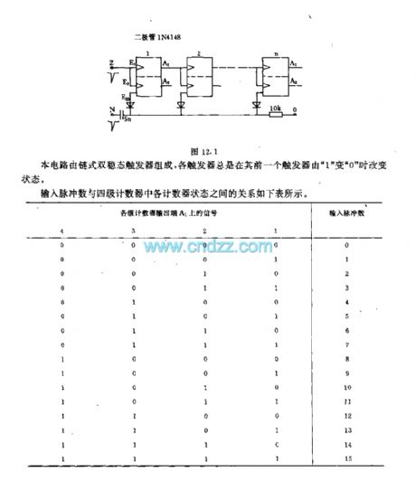
This circuit consists of chained flip flops, and each flip-flop change state when its former trigger changes from 1 to 0. The relationship between the input pulses and each counter status in four counters is shown in the table below.
(View)
View full Circuit Diagram | Comments | Reading(751)
Grating circuit for perforating and sampling
Published:2012/8/16 1:10:00 Author:Ecco | Keyword: Grating circuit , perforating , sampling
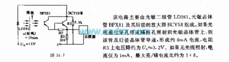
The circuit is mainly composed of the LD261 photodiode, phototransistor BPX81 and following connected amplifier BCY58. If the light is reflected to the phototransistor through the punched tape or bulkhead hole, the pipe and following connected transistor is conduction to form a current which is about 8mA, and voltage Ua on resistor R3 is about 3.2V. If there is no light irradiation, the current is only 1mA. The maximum bright, dark current ratio is about 1:8.
(View)
View full Circuit Diagram | Comments | Reading(680)
The interface circuit between single-chip accelerometer MMA1220D and microcontroller
Published:2012/8/15 21:27:00 Author:Ecco | Keyword: interface circuit , single-chip accelerometer , microcontroller
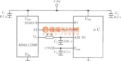
The microcontroller within A / D converter can use PIC MCU within A / D converter produced by the Microchip. MMA1220D's state end and self-test end are connected to the P1, P0 ports of μC, its output voltage is sent to the A / D converter input end. C1, C2 are the power supply decoupling capacitors. A / D converter's reference voltage side ( UREF ) is connected to +5 V power supply.
(View)
View full Circuit Diagram | Comments | Reading(1454)
The measuring infinitesimal displacement with optical emission components
Published:2012/8/15 22:49:00 Author:Ecco | Keyword: measuring , infinitesimal displacement , optical emission components

The 555 time-base circuit in the figure can generate oscillation signal, and it is added to the bistable multi -vibrator 4538 by photoconductive light-emitting diode and phototransistor, then it is shaped and output. Once there is a slight displacement makes the reflected light intensity change, the multivibrator will flip, then output signal UA changes, therefore the small displacement can be detected.
(View)
View full Circuit Diagram | Comments | Reading(1052)
The line mode acousto-optic voltmeter circuit with variable range of 1.2 to 1000V
Published:2012/8/15 22:53:00 Author:Ecco | Keyword: line mode , acousto-optic voltmeter , variable range , 1.2 to 1000V
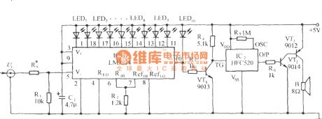
As shown in the figure, it is composed of the LED driver circuit, voice circuit, audio amplifier circuit, and it uses 10 LEDs to display linear voltage between 1.2 ~ 1000V, when the voltage is closed to the upper limit voltage, the circuit will issue a protected voice signal.
(View)
View full Circuit Diagram | Comments | Reading(1091)
Electrostatic detection of acousto-optic alarm circuit
Published:2012/8/15 22:59:00 Author:Ecco | Keyword: Electrostatic detection , acousto-optic alarm

The circuit is shown as the chart. It consists of electrostatic induction electronic switch and sound circuit. When the electrostatic field exists in the peripheral environment of computer, the circuit can detect the presence of static and issue the sound of beep , please attention , at the same time , the light-emitting diode will be lit to draw people's attention to the safe use of the computer or CPU chip.
(View)
View full Circuit Diagram | Comments | Reading(1415)
Thermistor electronic thermometer circuit diagram
Published:2012/8/16 22:17:00 Author:Ecco | Keyword: Thermistor, electronic thermometer

The thermistor RT and R1 , R2, R3 and RP1 form a temperature measurement bridge. When temperature is at 20 ℃, using R1, R3 and adjusting RP1 can allow bridge to keep balance. When temperature rises, the resistance of the thermistor RT reduces, the bridge in an unbalanced state, the imbalanced voltage output by bridge is amplified by operational amplifier, then the amplified imbalanced voltage causes corresponding deflection of microammeter connected to the op amp feedback circuit. The resistance of the thermistor is between 500 ~ 5000Ω.
(View)
View full Circuit Diagram | Comments | Reading(4199)
Low humidity detection circuit diagram composed of CGS ceramic humidity sensor
Published:2012/8/16 0:51:00 Author:Ecco | Keyword: Low humidity , detection circuit , CGS , ceramic , humidity sensor

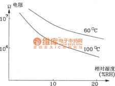

The op amp: μPC258CAnalog switch: TC4083BPThermistor: CTS-L (B=4100, Rr=3.08K, 100℃)
Moisture characteristic curve and the relativecurve at 60 ℃ and 100 ℃ are shown in the figure:
(View)
View full Circuit Diagram | Comments | Reading(1429)
The structure schematic of antimonide indium Hall elements
Published:2012/8/16 22:32:00 Author:Ecco | Keyword: structure schematic, antimonide indium, Hall elements
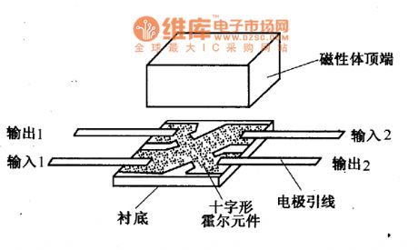
The figure shows the structure of antimonide indium Hall elements made by a sputtering process, and it consists of substrate, cross-shaped Hall element, electrode lead and the top of the magnetic body. In the leads of cross Hall element's four ends, one pair are current input ends, the other are the Hall voltage output ends. The top of the magnetic body is set in order to concentrate the magnetic field lines and the element sensitivity, and its volume of components is larger, the output sensitivity is higher.
(View)
View full Circuit Diagram | Comments | Reading(808)
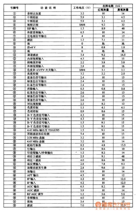
TDA8305A AGC and line / field scanning signal processing integrated circuit diagram
Published:2012/8/16 22:10:00 Author:Ecco | Keyword: medium , line , field scanning , signal processing, integrated circuit


TDA8305A is the image, AGC and line, field scanning samll-signal processing integrated circuit produced by Philips, and it is widely used in the Philips series of large-screen movements, color TVs.TDA8305A integrated circuit includes: image IF amplifier, AGC amplifier, AGC detector circuit, AGC control circuit; audio amplifier circuit, frequency discriminator, volume control, audio preamplifier circuit; sync separation circuit, phase detector circuit; line oscillation circuit, output circuit, X -ray protection circuit; field excitation circuit and its subsidiary circuits. Its internal block diagram is shown in Figure 1. TDA8305A IC uses 28-pin double row of plug-in package, and the pin functions and data are shown in Table 1.
(View)
View full Circuit Diagram | Comments | Reading(1979)
TV small-signal processing monolithic integrated circuit diagram
Published:2012/8/16 21:41:00 Author:Ecco | Keyword: TV , small-signal processing, monolithic, integrated circuit

DA8362 is the TV small-signal processing monolithic integrated circuit produced by Philips, which are widely used in a variety of import- brand and domestic large-screen color TVs.(1) Features and functionsTDA8362 IC includes image and audio signal processing circuit, line and field scanning signal processing circuit, chrominance and luminance signal processing circui, character display signal processing circuit, external video or luminance (Y) signal input circuit, sync separator and some other circuits with auxiliary functions. Its internal block diagram is shown in Figure 1.(2) pin functions and dataThe TDA8362 IC uses 52-pin dual in-line package, and pin functions and data are listed in Table 1.
(View)
View full Circuit Diagram | Comments | Reading(1791)
The microwave probe delay lighting circuit diagram with RD627
Published:2012/8/16 21:25:00 Author:Ecco | Keyword: microwave , probe , delay lighting
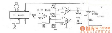
The microwave probe delay lighting circuit diagram with RD627 concistsofIC1, IC2 , and Triac VTH, and it is shown as the figure.
The internal circuit of IC1 is composed of oscillator , emission, amplifier, detector, limiter, delay and regulator circuits, and it has few external components, and loop antenna TX can be usedforemission and receiving. IC2 is usedas amplifier and comparator.
After the power is connected, antenna TX will launch the microwave signal out.When nobody comes intothe effective detection area ( an area of approximately 100m2), IC1's pin 6 outputs 6V, and IC2's pin 1 and pin 7 output low level, then diodes VD1 and VD2 are closed, the thyristor VTH is cut off because gate pole has no trigger voltage, and light EL is not bright.
(View)
View full Circuit Diagram | Comments | Reading(1079)
| Pages:367/2234 At 20361362363364365366367368369370371372373374375376377378379380Under 20 |
Circuit Categories
power supply circuit
Amplifier Circuit
Basic Circuit
LED and Light Circuit
Sensor Circuit
Signal Processing
Electrical Equipment Circuit
Control Circuit
Remote Control Circuit
A/D-D/A Converter Circuit
Audio Circuit
Measuring and Test Circuit
Communication Circuit
Computer-Related Circuit
555 Circuit
Automotive Circuit
Repairing Circuit