
Circuit Diagram
Index 372
AD603 voltage gain control circuit
Published:2012/7/23 2:42:00 Author:Ecco | Keyword: voltage gain control

This circuit uses two AD603 cascades to realize controllable gain range in 0 dB ~ 60 dB. AD603 monolithic gain range is 10 dB ~ 30 dB, and the range of input control voltage is 0 V ~ l V. Among them, the first-stage AD603 circuit diagram is shown as the figure. As AD603 input impedance is 100 Ω, it must add input buffer to improve the input impedance, then to meet the requirements of the system resistance. In addition, as the front-end circuit affects the noise of the circuit, the circuit uses the amplifier circuit composed of primary op amp AD620 as a pre- amplifier to reduce the noise.
(View)
View full Circuit Diagram | Comments | Reading(2889)
Infrared remote control dimming chandeliers circuit diagram
Published:2012/7/23 3:17:00 Author:Ecco | Keyword: Infrared , remote control , dimming chandeliers
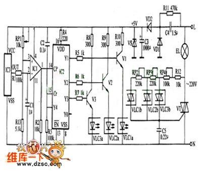
This infrared remote control dimming chandelierdescribed can use the remote controllerof household appliances ( such as TV, DVD player , VCR , etc. ) to control opening, turning off and dimming (3 files of strong, medium and weak light)of the lights.The working principle:The infrared remote control dimming chandelier circuitconsists of power circuit , IR receiver amplifier circuit and the dimming control circuit, and it isshown as the chart.
(View)
View full Circuit Diagram | Comments | Reading(3992)
The protection circuit composed of negative resistance LED
Published:2012/7/18 2:50:00 Author:Ecco | Keyword: protection circuit , negative resistance, LED

View full Circuit Diagram | Comments | Reading(860)
LED AC driver circuit
Published:2012/7/18 3:08:00 Author:Ecco | Keyword: LED, AC driver
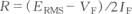
As shown in the figure, the circuit can work normally under the cases of unknown polarity of the voltage or power supply polaritybeing reversed or not. Being same with DC driver, the current limiting resistor values of R can de decided by the following formula when it is used as AC driver:
In the formula, ERMS is the effective value of AC voltage.
(View)
View full Circuit Diagram | Comments | Reading(1567)
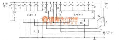
The bargraph display driver circuit with 20 light - emitting segments
Published:2012/7/18 3:25:00 Author:Ecco | Keyword: Bargraph display , driver , 20 , light - emitting segments
View full Circuit Diagram | Comments | Reading(1228)
LED power supply voltage-doubler circuit
Published:2012/7/18 3:23:00 Author:Ecco | Keyword: LED , power supply , voltage-doubler circuit

The power supply voltage-doubler conversion circuit is shown as the figure. Some amplifiers require small current and high voltage in electronic circuit designs, so the power supply voltage-doubler conversion circuit composed of flashing light-emitting diodes and a small number of components can be used. In Figure (a), the capacitors C1, C2 can be used to storage charge, and the circuit uses the oscillation of flashing light-emitting diode to drive relay switch for conversion, then C1 and supply voltage are superimposed to obtain twice of power supply voltage on C2. The output current of circuit is about 10mA. Relays uses 6V , 30mA types. The figure (b) is a voltage doubler schematic diagram.
(View)
View full Circuit Diagram | Comments | Reading(1558)
Blown fuse indicator circuit
Published:2012/7/18 3:01:00 Author:Ecco | Keyword: Blown fuse indicator
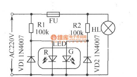
The blown fuse indicator circuit is shown as the figure. The LED -R is used to the AC power indicator, andLED -G is used the fuse FU status indicator. When FU is normal, two LEDs arelit,and the light isorange; after FU fuses, LED -G turns off, and only LED -R emits red light. The current limiting resistors R10, R2 can be replaced by the 220nF/450V capacitor,then the VD1, VD2 can be eliminating.
(View)
View full Circuit Diagram | Comments | Reading(2797)
BA313 sound recording or reproducing circuit diagram with ALC
Published:2012/7/16 3:15:00 Author:Ecco | Keyword: sound recording, reproducing , ALC
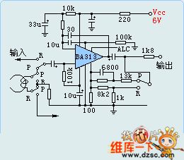
BA313 is a sound recording and preamplifier circuit with built-in automatic level control circuit (ALC), and it is commonly used in the cassette tape recorder. It is available in 9 -pin DIP dual in-line package. The circuit has the following characteristics : automatic level control with a wide range, wide working voltage range ( 3-12V ), high gain, low distortion, low noise.
(View)
View full Circuit Diagram | Comments | Reading(3567)
Stereo encoder circuit diagram with discrete components
Published:2012/7/16 2:53:00 Author:Ecco | Keyword: Stereo encoder , discrete components

View full Circuit Diagram | Comments | Reading(1068)
The power output circuit diagram with automatic drive mode
Published:2012/7/16 3:12:00 Author:Ecco | Keyword: power output , automatic drive mode

The output voltage of the system in the design is 3.3 V , and it uses automatic drive mode. It usesthe secondary of transformerto drive MOSFET. When the circuit works, the transformer's secondary is in positive hafle circle, V8 is breakover, V9 is turned off, and V8 plays the role of rectifying action. When transformer's secondary is in negative half cycle , V9is breakover, V8isturn off, V9 has the freewheeling function. As shown in Fig, when it works under the condition of 300 kHz , the loss of the synchronous rectifier is conduction loss, and the switching loss is small.
(View)
View full Circuit Diagram | Comments | Reading(978)
MCU control circuit diagram
Published:2012/7/16 2:52:00 Author:Ecco | Keyword: MCU control

The design of arbitrary waveform generator uses MATLAB's powerful simulation functions, and it can provide the frequency, cycle, pulse width of arbitrary waveform data conveniently and fastly; and data is stored in data memory. Under the control of the microcontroller, it uses CPLD circuit to generate and read the address. then the data is sent into the D / A converter circuit to get arbitrary waveform signal. The system block diagram is shown in Figure 1; The frequency dividing circuit and address generator is realized by the CPLD.
(View)
View full Circuit Diagram | Comments | Reading(965)
Voltage-controlled 4W audio amplifier circuit diagram
Published:2012/7/11 2:14:00 Author:Ecco | Keyword: Voltage-controlled , 4W , audio amplifier

Voltage-controlled 4W audio amplifier uses audio amplification IC TDA103Ato provide4W of output power. The control voltage is3.5 ~ 8V, and controlcharacteristic is logarithmic with controlling rangein 80dB.
(View)
View full Circuit Diagram | Comments | Reading(1432)
100W amplifier circuit diagram with DC 500KHZ
Published:2012/7/11 2:19:00 Author:Ecco | Keyword: 100W , amplifier , DC 500KHZ

The 100W amplifier with DC 500KHzuses the features of high input impedance , high gainofa photoelectric op amp to make output power be 100W. Load current can be up to 10A, and it requires high current wiring and capacitance power supply bypass . This circuit is used for high - fidelity audio circuits, cathode-ray deflection and servo system.
(View)
View full Circuit Diagram | Comments | Reading(2095)
ESL amplifier circuit diagram
Published:2012/7/11 2:11:00 Author:Ecco | Keyword: ESL amplifier

When the design shown in the figure is connected to the popular Stax 1 electrostatic headphones, it can transmit 200Vp - p voltage on full audio bandwidth. Although you can change the resistor divider to provide a bias voltage of up to 400VDC, the device shown in figure uses DC 200V bias. As many kinds of Stax headphones have similar driver and bias demands, the design also applies to these models.
(View)
View full Circuit Diagram | Comments | Reading(2189)
Impedance matching circuit diagram
Published:2012/7/11 2:07:00 Author:Ecco | Keyword: Impedance matching
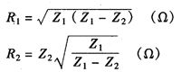
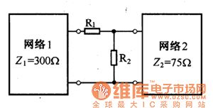
Figure 1 shows the impedance matching attenuator composed of resistor, andit is connectedbetween two networks with different impedance characteristic to play the role of matched impedance .Matching resistance in the devicecan be determined by following formula:
Z1 and Z2 areimpedance of the network 1 and network 2 , when they are respectively substituted into the above two formulas , then R1 = 259.8Ω, the R2 = 86.6Ω.
(View)
View full Circuit Diagram | Comments | Reading(1011)
Bistable multivibrator circuit diagram
Published:2012/7/11 2:00:00 Author:Ecco | Keyword: Bistable multivibrator


As shown in the figure, the circuitaretwo synchronized multivibrators composed of composed of two dualtime-base circuits 556, and itcan output two synchronous clock pulse signals, and the spacing and oscillation frequency can be changed by adjusting the time constant. It isflexibleand convenient. When you select C1 = C2 = C3 , the oscillation frequency is
.
The duty cycle D depends on R1 and R2, which can reach 5%~95%.
(View)
View full Circuit Diagram | Comments | Reading(1798)
Closed-loop three-phase multivibrator oscillator circuit diagram
Published:2012/7/11 1:37:00 Author:Ecco | Keyword: Closed-loop, three-phase multivibrator


As shown in the figure,the closed loop is composed of three identical Schmitt triggers connnectedend to end. Each trigger's delay timetd = l . 1 (RP + R) C,and td is the time required by voltage on C to rise to 1/3 VDD. After 555 resets, the charge on C is dischared by formerIC output ( pin 3 ) through R, W, and thus the charging time constant is the same with C's. Once each trigger circuit's output endneeds to change, it requires to be transmitted three single stable trigger circuits, and the required time is 3td Therefore, the output cycle of each IC Td = 6td . The corresponding frequencyis
(View)
View full Circuit Diagram | Comments | Reading(3713)
Rf driver audio oscillator circuit diagram
Published:2012/7/11 1:22:00 Author:Ecco | Keyword: Rf driver, audio oscillator

As shown in the figure, 555, Rl, RPland C1form thecontrolled audio oscillator , f = 1.44 / ( R1 +2 RP1) C1 , the icon parameter frequency isbetween 600Hz ~ 20kHz , and it can beselected by adjusting RP1.
(View)
View full Circuit Diagram | Comments | Reading(1967)
DC low-voltage blown fuse indicator circuit diagram
Published:2012/7/11 1:54:00 Author:Ecco | Keyword: DC low-voltage , blown fuse indicator

DC low-voltage blown fuse indicator circuit is shown as Figure 1, which consists of two light-emitting diodes VD2 , VD3 , a silicon rectifier diode VD1 and resistor R. When the fuse is good, the green light-emitting diode VD3 is bright. As the function of VD1 and VD3, the two ends' level of VD2 is equipotential, the red light-emitting diode VD2 is turned off. When the fuse is blown, VD3 it turned off as the cathode has no voltage, then the red light-emitting diode VD2 emits light as the influence of VD1 and R. According to the switching of VD2 and VD3, people can easily judge on-off status.
(View)
View full Circuit Diagram | Comments | Reading(2842)
Synchronized clock oscillator circuit diagram
Published:2012/7/8 21:23:00 Author:Ecco | Keyword: Synchronized clock oscillator

As shownin the figure, the controlled multivibrator iscomposed of 555 and R1, R2, C1, and the oscillation frequency is related to the RC time constant , but alsocan beadjustedby DC level of the control side. The DC level depends on the reference frequency f. After low-pass filter, the square wave is output by RS flip flop which is locked by oscillation frequency fo = Nfn output from 555. CD4001's two NOR gate circuits form the RS flip flop , when it is in a locked case , the duty cycle of the output will be kept, and thus the filtered DC level keepsconstant. If 555 oscillation frequency f0drift high(or fn reduces) , then the duty cycle will increase, thenthe DC control level will increase accordingly , frequency will decline; and vice versa.
(View)
View full Circuit Diagram | Comments | Reading(1524)
| Pages:372/2234 At 20361362363364365366367368369370371372373374375376377378379380Under 20 |
Circuit Categories
power supply circuit
Amplifier Circuit
Basic Circuit
LED and Light Circuit
Sensor Circuit
Signal Processing
Electrical Equipment Circuit
Control Circuit
Remote Control Circuit
A/D-D/A Converter Circuit
Audio Circuit
Measuring and Test Circuit
Communication Circuit
Computer-Related Circuit
555 Circuit
Automotive Circuit
Repairing Circuit