
Circuit Diagram
Index 362
LCD backlight brightness automatically control circuit ( visible brightness sensor LX1970 )
Published:2012/8/26 22:21:00 Author:Ecco | Keyword: LCD backlight , brightness, automatically control, visible , brightness sensor

When the ambient brightness is significantly dimmed, LX1970 can automatically open the LCD backlight to make white LED emit light. Automatic brightness control circuit is shown as the chart. The resistors R1 and R2 can be used to set the minimum and maximum values of controlling brightness. Changing the capacity of the capacitor C can adjust the response time and filter out the 50Hz mains interference. LX1970 uses +3.3 ~ +5 V power supply. If the circuit only uses SRC end, SNK end should be left vacant. Assuming driving white LEDs requires output voltage of 0.25 to 1.25V, 0.25V represents the minimum brightness of the LED, 1.25V represents the maximum brightness.
(View)
View full Circuit Diagram | Comments | Reading(1170)
White luminance measuring circuit composed of visible brightness sensor LX1970
Published:2012/8/26 22:44:00 Author:Ecco | Keyword: White luminance, measuring circuit, visible brightness sensor

UCC, current source and white-light LED form thelight sources which can emit visible light, and thevisible light isreceivedand transformed into a current signal by the LX1970. The SNK port, SRC port arerespectively connected with a micro-table in series to measure optical flowing ISNK, ISRC, and micro-table reading value reflects the level of brightness.
(View)
View full Circuit Diagram | Comments | Reading(965)
Brightness adjustment circuit with visible brightness sensor LX1970
Published:2012/8/26 22:50:00 Author:Ecco | Keyword: Brightness adjustment , visible brightness sensor
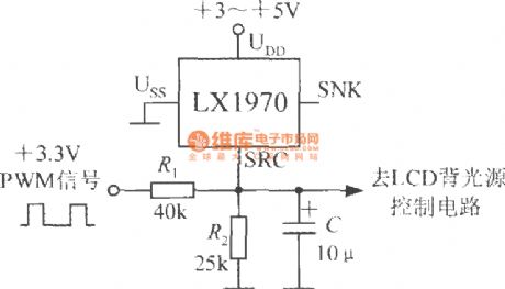
It only needs to change duty cycle of PWM (pulse width modulation) signal, the backlight brightness can be adjusted to suit individual needs. PWM signal voltage range is 3. 3V.
(View)
View full Circuit Diagram | Comments | Reading(552)
Smoke alarm circuit composed of photoelectric smoke detection IC MC145010
Published:2012/8/26 22:48:00 Author:Ecco | Keyword: Smoke alarm , photoelectric, smoke detection IC


It uses 9V laminated battery. R2, C3 are respectively Oscillation resistor and oscillation capacitor, and the clock cycle is decided by following formula:
(View)
View full Circuit Diagram | Comments | Reading(1703)
Wireless responder circuit with transceiver and codecs module
Published:2012/8/26 21:40:00 Author:Ecco | Keyword: Wireless responder , transceiver , codecs module

Transmitter circuit is mainly composed of radio transmission header TDC1808 and dedicated coding integrated circuit MC145026, and it is shown in Figure 1. MC145026 encoding manifold's pin function is shown in Figure 2. It consists of the clock oscillator, divider, address/data-encoding input circuit and data selection and buffer. Clock oscillator and divider provide benchmark clock for the whole encoder to coordinate the work of other parts. Address/data-encoding input circuit will enter different addresses and encoding signals converted from data. Data selection and buffer circuit can change parallel code to a serial code and output.
(View)
View full Circuit Diagram | Comments | Reading(1834)
1.5V miniature wireless FM microphone circuit
Published:2012/8/26 21:03:00 Author:Ecco | Keyword: 1.5V, miniature , wireless , FM microphone
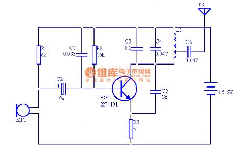
The circuit shown in this paper uses 12 components to form a miniature wireless FM microphone with stable operating frequency, and its transmitting distance is about 30 meters and more than 100 meters at 6V power supply.The circuit is shown as Figure, BG1, C1 and C3 form a high - frequency oscillation circuit. The transmitting distance is related to the current of the launch tube, and the upward bias resistor R2 can change BG1 output current.If you select BG1, tube's fT must be greater than 300MHz, but if the fT is too high, it will affect modulation. Inductance L uses two coils to make wound, but the wound must be the same, L1 uses 0.5mm enameled wire with 4 turns in a diameter of around 5mm-diameter skeleton, L2 has 3 turns. The antenna can be made by a soft wire with 0.6 meters length.
(View)
View full Circuit Diagram | Comments | Reading(7119)
Power polarity tester
Published:2012/8/24 22:46:00 Author:Ecco | Keyword: Power polarity, tester

This circuit can detect positive and negative polaritywith the power supply between 3V-30V and LED indicator. The test circuit is a constant current source. When the polarity of inputmeasured power iscorrect, T1 , T2are also turned o , the LED emitslight. The diode D2 allows T2 base voltage to maintain constant current . Thus, regardless of the size of conduction currentfromT1, T2will substantially send constant current. If the measured powerhas opposite polarity, the diode D1 is turned on, T1, T2 arecut off, LED goes out , the switch S1 can self-test the internal circuit of LED.
(View)
View full Circuit Diagram | Comments | Reading(1723)
Line status indicator
Published:2012/8/24 22:39:00 Author:Ecco | Keyword: Line status, indicator
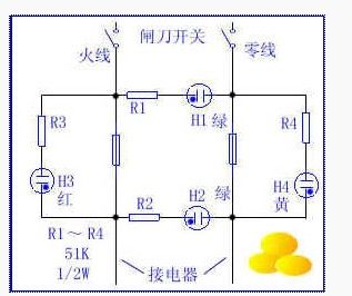
As shown in the figure, when the circuit is normal, H1, H2 glow, H3, H4 is not lit. When fuse on power line is blown, H3 is lit and H2 is extinguished. When the fuse on zero line blows, H4 is lit, H2 is extinguished. When two fuses are blown, H2, H3 , H4 are turned off, H1 is still lit. When H1, H2 shine, the applicance can not work properly, it shows that the device or the line after H2 is in failure. When fuse blows at night, H1 is also available for indoor shimmer lighting, allowing users to replace the fuse safety.Production: neon can use the neon bulb in fluorescent starter, its power consumption is minimal. If the neon bulb is pasted colored paper, it is easier to observe.
(View)
View full Circuit Diagram | Comments | Reading(1280)
Burn-in circuit with aluminum electrolytic capacitor
Published:2012/8/24 21:36:00 Author:Ecco | Keyword: Burn-in circuit , aluminum electrolytic capacitor
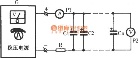
The burn-in of electrolytic capacitors is an effective way to reduce its leakage current. Burn-in method is shown as the figure. In the figure, G is a regulated power supply voltage, and its maximum current is above 1.5A. P1 is DC milliammeter with above 500mA range; P2 is DC voltmeter which is sectected according burn-in voltage value. The R -limiting resistor: resistance is selected by burn-in capacitor rated working voltage with 1V taking 1Ω. If the burn-in capacitor rated voltage is greater than 100V, R take, 1kΩ, the power of resistor R should be greater than 2W, depending on the value of parallel capacitor.
(View)
View full Circuit Diagram | Comments | Reading(1550)
Working performance test circuit of three-terminal regulator IC
Published:2012/8/24 21:47:00 Author:Ecco | Keyword: Working performance, test circuit, three-terminal regulator IC

Three terminal regulator's pin ① and pin ② are added DC voltage (it uses adjustable DC Power G in Figure), but people must pay attention to the polarity of G , Ui should be at least higher 2V than regulator regulator value U, but the maximum should not exceed 35V. When multimeter is in DC voltage block to measure the voltage between pin ③ and pin ②, the value is stable voltage of the regulator. (View)
View full Circuit Diagram | Comments | Reading(1088)
Three - phase power supply phase sequence / open phase detector
Published:2012/8/24 22:28:00 Author:Ecco | Keyword: Three - phase , power supply , phase sequence, open phase, detector

It is mainly used to detect the three-phase AC power wiring with phase loss and correct phase sequence or not. Circuit schematic is shown in thefigure, in the figure, if the A -phase ( 1 ), C phase ( 3 ) , B phase ( 2) are respectively connected to the thyristor A , G, and K electrode, thyristor T will get conduction in singlephase half cycle, the light - emitting diode will emit normal light, when the three-phase phase sequence of connections A, B, C is incorrect, the conduction time of the triac T will become shorte , the average current decreases and LED brightness is also greatly reduced.When one or two phasesaremissed inthe three-phase AC, SCR iscut off, LED goes ou, the values of R3, R4 and C will determine the length of the delay time t.
(View)
View full Circuit Diagram | Comments | Reading(7360)
Interface circuit of sample and hold amplifiers AD781 and AD674
Published:2012/8/24 21:48:00 Author:Ecco | Keyword: Interface circuit , sample and hold , amplifier
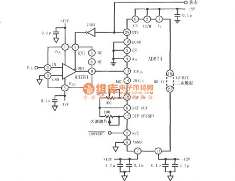
View full Circuit Diagram | Comments | Reading(1060)
The basic connection circuit of sample and hold amplifier AD9101
Published:2012/8/24 22:00:00 Author:Ecco | Keyword: basic connection , sample and hold , amplifier
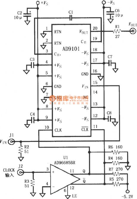
AD9101 is built-in the holding capacitor CHOLD, and sample-and-hold is controlled by the CLOCK. According to basic connection diagram, RTN grounds to keep the gain of the amplifier in 4. The noninverting input terminal of ultrafast comparator AD96685BR produced by the Analog Devices Inc. is added the clock input, then Q is sent to AD9100's non CLK and CLK (10,11 feet) as the sampling and holding control signal. The capacitors without marking use 0.01μF; the selection of R1 should be subject to the load capacitor with considering the condition that load capacitance may be less than 6pF in short circuit.
(View)
View full Circuit Diagram | Comments | Reading(1314)
Two-channel switch circuit with sample-and-hold amplifier LF398
Published:2012/8/24 22:17:00 Author:Ecco | Keyword: Two -channel, switch , sample-and-hold, amplifier
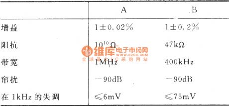
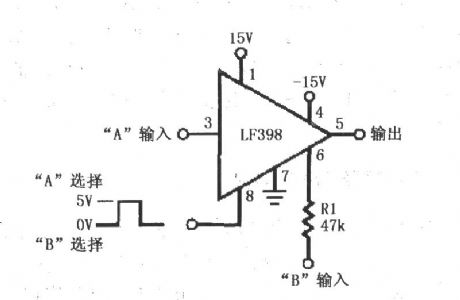
Two input signals A, B are respectively added to the input end ( pin 3 ) and sampling capacitor end ( pin 6 ), pin 8 is connected to selecting pulse, and the internal switch can be used to change channels A and B, when a pulse is high (5V ), the internal switch is closed, the output is the A channel signal; when the selection pulse is low (0V), the internal switch is turned off, the signal output is the B channel. The parameters of the channel A, B are shown in the table below.
(View)
View full Circuit Diagram | Comments | Reading(3352)
The GPS receiver downconverter circuit with MAX2682
Published:2012/8/25 1:29:00 Author:Ecco | Keyword: GPS receiver , downconverter
The typical application circuit of MAX2680/MAX2681/MAX2682 is shown as following:
(View)
View full Circuit Diagram | Comments | Reading(1050)
RF2498-based GPS receiver downconverter circuit
Published:2012/8/25 1:53:00 Author:Ecco | Keyword: GPS receiver , downconverter

RF2498 is a high-performance CDMA band / dual mode integrated LNA / mixer circuit, a three- band LNA / downconverter. RF2498 can be used in CDMA / Cellular / PCS / GPS handheld devices, JCDMA / GSP handheld devices, CDMA modems / data cards, commercial and consumer systems, portable batteries. RF2498 meets the requirements of IS-98 sensitivity, interact modulation and tone adjustment. RF2498's gain control is 29dB in the PCS band and gain control 27.5dB in cellular band. RF2498 provides 37dB gain for a GPS LNA / mixer application. The RF2498 uses three-state gain control mode to meet the IS-98 IMD test. The chip has an integrated TX LO buffer.
(View)
View full Circuit Diagram | Comments | Reading(1956)
μPB1009K - based GPS receiver RF front-end circuit
Published:2012/8/25 1:28:00 Author:Ecco | Keyword: GPS receiver , RF front-end
μPBl009K is a single-chip GPS receiver chip which integrates full VCO, the second stage IF ( intermediate frequency ) filter, 4bit ADC, digital control interface circuit.μPBl009K has the double conversion function: fREFin = 16.368 MHz f1stFin = 61.380MHz f2dFin = 4.092 MHz ; fREFin 14.4/16.384/19.2/26MHz f1stFin = 62.980MHz f2ndIFin = 2 . 556MHz. It has a multi - system clock. With frequency divider ( 1 / N = 100,3 / 256,9 / 1024,65 / 4096 ) on the conversion sheet, TCXO frequency can be 16.368MHz/16.384MHz, 14.4MHz, 19 .2 MHz, or 26MHz. The power supply voltage Vcc = 2.7V - 3.3V. Low current consumption : lcc = 26.0mA.μPBl009K can be applied to the GPS receiver with reference frequency in 16.368MHz, the second-stage IF frequency in 4.092MHz, and the GPS receiver with reference frequency in 14.4MHz , 16.384MHz, 19.2MHz and 26MHz, the second-stage IF frequency in 2.556MHz.
(View)
View full Circuit Diagram | Comments | Reading(2392)
GP2015 - based GPS receiver RF front-end circuit
Published:2012/8/25 1:10:00 Author:Ecco | Keyword: GPS receiver, RF, front-end


The GP2015 is a GPS receiver RF front-end circuit which provides a low- power, low-cost and high reliability GPs RF front-end solution. With the same performance of GP2010, GP2015 uses TQFP-48 package, 3V to 5V operating supply voltage, 200mW (3V voltage) power consumption. Ll (1575.42MHz) C / A (Coarse-Acquisition) code signal is input to GP2015 by the antenna and low noise amplifier to output is a 2bit digital signal. The GP2015 includes an on-chip synthesizer, mixer, automatic gain control (AGC), and a quantizer which can provide sign and magnitude digital output. A complete GPS receiver RF front-end circuit only requires minimal external components.
(View)
View full Circuit Diagram | Comments | Reading(2271)
GPl020-based 6-channel correlator circuit
Published:2012/8/25 1:21:00 Author:Ecco | Keyword: 6-channel correlator
GPl020 is a 6-channel CMOS digital correlator which can be used with GPl010 L1 channel down converter or other integrated circuit to intercept and track the GPS C / A code or GLONASS code. Each channel of 6 channels in GPl020 includes: separate digital downconverted to baseband processing circuit, C / A code generator, correlator and accumulation dump register. GPl020 connects to the interface of a microprocessor by a 16-bit data bus, and it uses different on-chip registers to control the process of acquisition and tracking. The input multiplexer is suitable for GPS front end and GLONASS front end, allowing antenna differences. Supply voltage of the circuit is 5v, power consumption is less than 500mW, and it is available in 120L MQFP package with size in 28mm × 28mm × 3.4mm.
(View)
View full Circuit Diagram | Comments | Reading(1301)
MAX2641-based GPS receiver LNA circuit
Published:2012/8/25 1:14:00 Author:Ecco | Keyword: GPS receiver, LNA
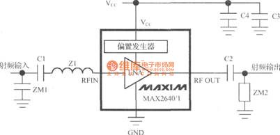
The MAX2641 is alow-price, ultra - low noise LNA whichcan be used in cellular phones, PCS, GPS, and 2.4GHz ISM band.With single-ended power supply, thevoltage is +2.7 V to +5.5 V , the current consumption is 3.5mA.
MAX2641's frequency rangeis 1400MHz ~ 2500MHz, typical gainis 15.7dB, the input IP3is 4dBm, noise figureis 1.2dB at 1575MHz. MAX2641 usesinternal bias circuit without external bias resistors and chokes. It requires the input matching network withonly two components,input / output blocking capacitor and VCC bypass capacitor. It is available in SOT23-6 package.
(View)
View full Circuit Diagram | Comments | Reading(1598)
| Pages:362/2234 At 20361362363364365366367368369370371372373374375376377378379380Under 20 |
Circuit Categories
power supply circuit
Amplifier Circuit
Basic Circuit
LED and Light Circuit
Sensor Circuit
Signal Processing
Electrical Equipment Circuit
Control Circuit
Remote Control Circuit
A/D-D/A Converter Circuit
Audio Circuit
Measuring and Test Circuit
Communication Circuit
Computer-Related Circuit
555 Circuit
Automotive Circuit
Repairing Circuit