
Circuit Diagram
Index 382
Switching voltage regulator of Jinxin brand TV
Published:2011/11/14 3:33:00 Author:May | Keyword: Switching voltage regulator, Jinxin brand TV

Switching power supply with input and output isolation normally has three forms: transformer isolation, photoelectric coupling isolation and sampling and output segregating isolation.
Switching voltage regulator of Jinxing brand is shown in the diagram. It adopts two transformers. Sampling circuit R1, Rp and R2 directly connect to the output end of power supply. It can sample from 120V output voltage to a scale and add to the base of error amplifier VT1. This voltage and the reference voltage offered by VD1 and R5 are compared and enlarged by VT1. Then the collector is outputting error voltage. It is direct coupled by R7 and giving it to pulse width modulation circuit composed of Schmidt trigger VT2 and VT3. Then it is changed to pulse. The pulse is enlarged by VT4. It can realize total isolation except switching output stage. Its sound insulation is perfect. What’s more, we should use a transformer T1.
(View)
View full Circuit Diagram | Comments | Reading(1193)
Jinxin C7428 power supply
Published:2011/11/21 20:40:00 Author:May | Keyword: Jinxin, power supply

C7428 power supply adopts wide voltage design. It can adapt 110V-245V network voltage. It is similar to Toshiba 2500XH power supply.
Network input switching circuit
In order to adapt11V-245V network voltage, this power supply is designedfor freely switch over voltage multiplying rectifier and bridge rectifier. The power supply adopts multiplying rectifier when network input voltage is lower than 145V. It adopts bridge rectifier when network input voltage is higher than 145V.
Network input voltage is firstly rectified by V801, V802to get identification voltage on C808 after low-pass filtering. The identification voltage is added to STR81145's pin 2, 5. If network input voltage is lower than 145V, thevoltage on thetwo ends of C808 is lower. STR81145's pin 2, 3are breaked over. At this time, V803 and C818, C819 make up multiplying rectifier. The circuit has over voltage protection circuit in order to prevent STR81145's error identification. (View)
View full Circuit Diagram | Comments | Reading(1816)
Simple ringing choke type switching stabilized voltage supply
Published:2011/11/21 21:19:00 Author:May | Keyword: ringing choke type, switching, stabilized voltage supply

Ringing choke type is a kind of self-oscillation feedback converting model. Its basic principle is shown in the diagram. When it adds input power supply, the current passes Rg and flows to the base of switching tube VT1 to make VT1 break over. At this time, thediode of transformer secondary polarity is in reverse bias. The diode has no current. So the current of VT1 collector and transformer winding Np is the same. Rg is called starting resistor.
Once VT1 is breaking over, transformer primary winding Np is added input voltage, and coil NB also generates induction voltage UB. Also, coil NB adds current IB to the base of VT1to make VT1 further breaking over.
Transformer generates electromotive force, of which the polarity is the contrary of input voltage's polarity. When VT1 is cutting off, its power is the samewith thetransformer before VT1 is cut off.
The diode of transformer secondary polarity is breaking over due to the function of reverse electromotive force. The power transformer stored in unit time is equal to output power. (View)
View full Circuit Diagram | Comments | Reading(3212)
Reduced voltage type chopping type switching stabilized voltage supply principle diagram
Published:2011/11/14 0:26:00 Author:May | Keyword: Reduced voltage type, chopping type, switching stabilized voltage supply

Chopping switching stabilized voltage supply is DC energy supply. It can get single-direction square wave after passing switching circuit. Then it can get stable DC which is different with input voltage after filtering. Soit means that whether input voltage Ui is positive or negative, output voltage Uo is always lower than input voltage Ui, that is | Uo|≤|Ui|. The diagram shows reduced voltage chopping type switching stabilized voltage supply principle diagram. When switching component VT is controlled and saturation conduction, the energy is stored in inductor L and capacitor C. When switching component T is controlled and in the cut-off state, the energy stored in inductor and capacitor is still offered to load, and the diode CD makes up the current loop. It is also called series switching stabilized voltage supply because switching component VT and load resistor RLare connected inseries. (View)
View full Circuit Diagram | Comments | Reading(820)
High voltage switching stabilized voltage supply circuit
Published:2011/11/13 21:48:00 Author:May | Keyword: High voltage, switching, stabilized voltage supply

High voltage switching stabilized voltage supply circuit is shown in the diagram. It is the switching power supply of 80P type color TV. It adopts auto-excitation, PWM circuit. Its output is isolated with power system. This power supply has 110V and 18V DC voltage output. The power supply consists of power frequency rectification filtration circuit, start oscillating circuit, control circuit and DC output circuit.
Input filter composed of capacitors C309, C301 and inductor L301 to weaken the power system interference of power supply. It also can prevent power supply from interfering and polluting. Power frequency rectification filtration circuit composed of VD301~VD304 tochange 220V AC voltage into about 300V DC current. The usage of C304~C307 is to protect the diode form being parallel with them. 300V DC voltage passes starting resistor R302 to reduce voltage, then it will be added to the base of switching compensating pipe VT304, which canmake it to get positive bias and turn on. At the same time, the end of input winding ⑨~② pulse transformer T301 has current. It makes feedback winding 11~⑩ end get positive feedback. (View)
View full Circuit Diagram | Comments | Reading(3068)
Non-resonance converter circuit
Published:2011/11/14 1:08:00 Author:May | Keyword: Non-resonance, converter
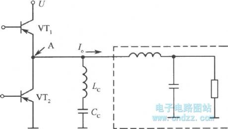
The inductance current commutating mode converter is seldom occuring the phenomenon of surge, even if it adopts non-resonant mode to zero voltage switch in principle. Moreover, it can adjust the voltage by PWM control. The diagram is the basic circuit of this mode. Lc is inductance when changing current. Cc is the capacitor (not for non-resonant use) to cut off DC. Under this mode, VT1 and VT2 will turn on and cut off in turns. Among the turning on and cut-off time, the two switches have cut-off time. In this period of time, the power of inductance LC will charge and discharge to the capacitor between drain-source of VT1 and VT2. It can make A point voltage drop to zero or equal to power supply voltage U before next on-off cycle. So it can reach the zero voltage on-ff condition, at the same time, it also controls the surge current.
(View)
View full Circuit Diagram | Comments | Reading(721)
Single-ended Foward Transforming Switching Regulated Power Supply Application Circuit
Published:2011/11/13 21:55:00 Author:May | Keyword: Single end, positive energize, converter type, switching, regulated power supply

The diagram is single-ended Foward Transforming Switching Regulated Power Supply Application Circuit. The isolation effect is good because it adopts photo-coupler in the feedback loop. The output voltage of this power supply is 5V. The output current is 10A. When the power supply is broken over, it will output 300V DC voltage through the rectifying and filtering of VD1, L1, C1. It is added on switching tube VT1 directly, and it will provide a working voltagefor control circuit tomake it work.
During the switching tube VT1 is breaking over, the secondary winding N2 of transformer T gets energy. Its polarity can make rectifier diode VD3 breakover.
When output voltage Uo is increasing due to some reasons, the current of VT4, VT5 is increasing. This current is coupling to VT2 through photo-coupler VT3, it can decrease the internal resistance of VT2, thereby the base potential of control switching tube VT1 is decreasing, VT1's duty factor is decreasing, Uo is dropping down.
(View)
View full Circuit Diagram | Comments | Reading(952)
Single end positive energize converter type converting circuit
Published:2011/11/14 3:30:00 Author:May | Keyword: Single end, positive energize, converter, converting
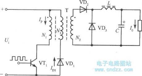
The typical structure of Single end positive energize converter type converting circuit is shown in the diagram. Its circuit form is almost the same as single end negative energize converter. But its working conditions is quite other. When switching transistor VT1 is breaking over, transformer secondary polarity's rectifier diode VD2 is breaking over, and at this time, network is delivering energy to load, and filter inductance L is storing energy; when VT1 is cutting off, inductor continues to release energy to load through fly-wheel diode VD3. It must use clamping winding in single end positive energize converter. The function of clamping winding is to limit the voltage peak on the collector of transistor and make the magnetic flux of high frequency to reset. In general, the turn number of clamping winding is equal to primary winding, and it should close coupling with it. Due to the function of clamping winding, switching transistor VT1's highest back voltage is limiting in two times power supply voltage. At this time, in order to satisfy the condition of magnetic core reset, namely the building time and resetting time of magnetic flux is the same, so the duty factor of this circuit must less than 50%. (View)
View full Circuit Diagram | Comments | Reading(626)
UM3758 Infrared or ultrasonic remote-controlled transceiver amphibious circuit
Published:2011/8/30 21:32:00 Author:Jessie | Keyword: infrared, ultrasonic, remote-controlled
Technical characteristics:Using CMOS technology, low power consumption.Easy to link to other CMOS technology integrated circuits.Working voltage range is wide, and its value is 3 ~ 12 V.Containing RC clock oscillating circuit.Using mask choice to form series products.
(View)
View full Circuit Diagram | Comments | Reading(3007)
Practical power supply of single end fly back type switching regulated power supply
Published:2011/11/14 3:29:00 Author:May | Keyword: single end, fly back type, switching, regulated power supply

The following diagram is a practical power supply of single end fly back type switching regulated power supply. It adopts CW3840 pulse width modulation integrated circuit to control. At present, CW3840 is pulse width modulation with many functions. Its internal circuit including precise power supply, oscillator, error amplifier, over voltage and over current comparator, slop generator, pulse width modulation and slow starts and program control circuit, etc.
AC main supply voltage 220V (or 110V) passes bridge rectifier VD1 to rectify and C1, C2 to filter. Then it will generate 300V DC voltage. The voltage pass resistor R3, R4 to reduce voltage. Then it will add to CW3840's 15 end and as working voltage. CW3840's working voltage slowly increased to 12V because of capacitor C3. This voltage passes R7, R8 to divide voltage and add it to 2 end of over voltage comparator. The threshold value of this comparator is 3V. When 2 end voltage is less than 3V, comparator outputs low level. It can make the drive transistor on integrated circuit cutting off and starts latch is locking. It indicated under voltage error. It also makes 8 end and capacitor C9 to be low level. Protective power supply is slow starting.
(View)
View full Circuit Diagram | Comments | Reading(1071)
TOP209/210 pin configuration
Published:2011/11/14 3:22:00 Author:May | Keyword: pin configuration

TOP209/210 series is a kind of highly efficient, low-power, pulse width modulated type three-terminal chip switching power supply successfully developed by Power Company in 1997 and is suitable for Stand-by Power of small power switching power supply with less than 8W power or electrical equipment.
TOP209/210 has two kinds of package: 8 foot dual inline (DIP-8) and 8-pin surface mount (SMD-8). Pin configuration is shown in the diagram. It is still equivalent to three-terminal devices because pin 2,3,6,7 all are empty (NC). Pin 1 and pin 8are connected inside. The only difference is pin 1 is connected with external bias / feedback Back to bypass capacitor terminal and control the negative side and pin 8 is external connected with high back end of the primary grade (HVRTN) when designing PCB. Pin 4 is connected with control end and pin 5 is connected with drain end. Its working principle is the samewith TOP100. But we must explain that: (1) TOP209's switching frequency is changed to 70kHz, and the switching frequency of TOP210 is still 100kHz; (2) both ofthe thermal shutdown temperatureis 145°C, and it is 10°C higher than TOPSwitch - Ⅱ's; (3) TOP209/210's limiting current values separatelyare 0.15 ~ O.23A, 0.23 ~ 0.30A; (4) Power MOSFET's withstand voltage is 700V.
(View)
View full Circuit Diagram | Comments | Reading(1373)
Multistage timing program control circuit with CD4017, LM555
Published:2011/8/30 1:50:00 Author:Jessie | Keyword: Multistage timing, program control

This program control circuit has tenth level program control output.Each level program can set timing time according to the actual need of work. Also, according to the actual control needs, it can be arbitrarily selectedin ten level. Circuit structure is simple, reliable, economical. Circuit components areas shown, there are only program pulse splitter and regular controller. (View)
View full Circuit Diagram | Comments | Reading(1999)
Differential input/output gain programmable amplifier circuit
Published:2011/8/30 21:23:00 Author:Jessie | Keyword: Differential input/output, gain programmable, amplifier


As shown in the chart, the circuitis thedifferential input/output gain programmable amplifier circuit. This circuit is composedof two pieces of PGA202 integrated circuits. PGA202 is mosfet input instrument integrated amp, and its gain has four different values: 1, 10, 100 and 1000. In circuit A0 (pin 1) and A1 (pins 2)are gain control terminals. when A0 and A1 are at different levels ( 1 or 0 ),their gainvalues aredifferent. Because here is two amplifier circuits using parallel form, thus circuits' total gain is twice of the monolithic gain , namely Vo = 2Av1Vi. Av1 ismonolithic amplifier circuit's gain, so the circuit's total gain is Av2 = 2Av1. CorrespondingAv2's valuesalso have four: 2, 20, 200, 2000. The relationship betweenthe total gain Av2 and gain control ports A0, A1 is listed in table. (View)
View full Circuit Diagram | Comments | Reading(837)
ZVT soft-switching PFC switching regulated power supply circuit
Published:2011/11/14 2:42:00 Author:May | Keyword: ZVT soft-switching, PFC, switching regulated power supply


The diagram is power factor adjustment (PFC) switching regulated power supply circuit using zero-voltage converter (ZVT) soft-switch technique. Compared with hard switching active power factor adjustment (PFC) circuit, this circuit has one more out of auxiliary switch tube and resonant circuit. Main switching tube VTr and auxiliary switch VTr1 can becontrolled by a piece of IC chip-UC3855AN.
In the diagram, auxiliary switch and resonance LC circuit can make main switch tube achieve ZVT soft switch working. UC3855AN outputs two ways pulse trains, and they separately control the turning on of main switch tube and auxiliary switching tube. The computation of its feedback sampling and duty factor is the similar to UC3854.
The internal structure of UC3854 single chip integrated circuit is shown in the following diagram. It mainly consists of voltage amplifier, analog multiplier, current amplifier and the composition of fixed-frequency pulse width modulator. in addition, it contains gate driver which is compatible with power MOSFET, 7.5V voltage reference, load enabling comparators, voltage detection and over-current comparator. UC3854 can accurately keep the sine ratio of bus input current with no need to slop compensation to the current.
(View)
View full Circuit Diagram | Comments | Reading(1708)
Switching regulated power supply using 110V (doubling voltage)/220V AC voltage input
Published:2011/11/13 21:33:00 Author:May | Keyword: Switching regulated power supply, 110V (doubling voltage)/220V AC voltage input

This power supply circuit is shown in the diagram. Its input AC voltage is 110V or 220V. When 110V AC voltage power supply changesin the range of 85~132V or 220V AC voltage power supply changes at the range of 170~265V, Sv=±1%. When the changing range of load current is 10%~100%, Si=5%, output ripple voltage is ±50mV. S in the circuit is 110V/220V AC voltage option switch. It can use cable jumper on printed plate to replace switch. When S is closed, it chooses 110V AC voltage as input, at this time, voltage doubling rectifying circuit consists of rectifying bridge BR and resistor capacitor components R1, C1, R2 and C2. When S is cut, it chooses 220V AC voltage as input. It added resistor R4 in output circuit in order to improve the voltage stability when it is atlight load. The smallest load current set by it is 36mA.
(View)
View full Circuit Diagram | Comments | Reading(3363)
Used for floating-point transform gain variable buffer amplifier circuit
Published:2011/8/31 1:14:00 Author:Jessie | Keyword: floating-point transform, gain variable, buffer amplifier

As shown in figure, the circuitis floating-point transform gain variable buffer amplifier circuit. The circuit consists of two parts: the buffer amplifier composedof OPA676 and theA/D conversion interface circuitcomposedof ADC603. OPA676 integrated chip's internal has two characteristics identical but independent differential amplification input levels. The two channels A and B can realize strobe by choosing pin 12's level. That is, when pins 12 is ata high level, channel A works, channel B cuts off; When pin 12 isat a low level, channel A cuts off, channel B works. The two channels' gains are different, using pin 12'scorresponding chose can realize gain's choice. We can learn from the diagram: Channel A voltage magnification is AVA=1+R2/R1=2; Channel B's voltage magnification is AvB=1+R4/R3=1+412/59=8. (View)
View full Circuit Diagram | Comments | Reading(950)
Switching power supply of Beijing brand black and white TV
Published:2011/11/13 21:28:00 Author:May | Keyword: Switching power supply, Beijing brand, black and white TV

The diagram shows switching regulated power supply of Beijing brand white and black TV. It is a typical example of low voltage switching regulated power supply.
This power supply has three ways of DC output that is 18V, 28V and 12V. Among them, 28V is directly outputted by bridge type rectifier; 12V is output after 28V voltage beingregulated by switching voltage regulator; 18V is output by half wave rectifying and filter circuit.
VZ601 is switch power adjustable tube. Self-excited harmonic oscillator consists of VT601~VT603, R601, C601, etc. This power supply belongs to pulse width modulation type switching regulated power supply. When 12V voltage isincreased because of some reasons, the base potential of error amplifier tube VT601 is increased. Its collector potential is decreased, base potential of VT603 is also decreased, the output pulse width of switching adjustable tube VT601 is narrow, it makes increased voltage decreased again. (View)
View full Circuit Diagram | Comments | Reading(1335)
400MHz differential amplifiering circuit
Published:2011/8/30 2:49:00 Author:Jessie | Keyword: differential amplifier

As shown in figure, the circuitis 400MHz broadband differential amplifying circuit. This circuit consists of two parts: the input broadband differential amplifier of integrated chip OPA660 and the caching amplifying circuit composedof BUF601. This circuit's voltage magnification is: Av=R9/(R8+1/gm), gm is the transconductance OPA660's transconductance amplifier OTA. Because in the chart the resistance R10=560Ω, OPA660's static current is about 10mA, at this timethe transconductance is gm=82mA/V. (View)
View full Circuit Diagram | Comments | Reading(703)
Simplified principle diagram of non-isolation switching power supply
Published:2011/11/13 21:21:00 Author:May | Keyword: non-isolation switching, power supply

In high-voltage switching power supply, it cancels power frequency transformer with isolation effect, and it isshown in the diagram. It is simplified principle diagram of switching power supply which is non-isolation with network. Switching tube VT1 is connectedto network through rectifier, the switching tubehas electrification. Switching tube can couple the energy to output end through high-frequency transformer. Because output end and input end have the same earth point andare directly connected with error amplifier VT2 connected in output end and switching tube VT1, output end is breaking over with network through output end. (View)
View full Circuit Diagram | Comments | Reading(1278)
Power supply controller with high efficiency under various load condition
Published:2011/11/13 21:13:00 Author:May | Keyword: Power supply controller, high efficiency, under various load condition


Aimed at all sorts of AC/DC and DC/DC conversion applications, iWatt company has developed three kinds of chip which can achieve pulse Train technology. The company also integrates some other functions in it. The functions are control logic, waveform analyzer, multiplexer, regulators and drives and so on. iW2101 is isolation DC / DC controller chip; iW2201 is AC / DC controller chip; iW2202 is single-chip type AC / DC controller with internal active PFC circuit.
Differ from other PFC program using complex circuits and common PWM controller, the FPC and regulated voltage of iW2202 are both offered by the initial feedback of single-stage single-switch topology, as shown in Figure 4. In the same application, the other PFC programs can make the justified voltage of capacitor over 1000V, but iW2202 program does not exceed 400V. It can not only reduce the stress of component and improve reliability, but also can achieve higher performance at lower cost systems.
(View)
View full Circuit Diagram | Comments | Reading(670)
| Pages:382/2234 At 20381382383384385386387388389390391392393394395396397398399400Under 20 |
Circuit Categories
power supply circuit
Amplifier Circuit
Basic Circuit
LED and Light Circuit
Sensor Circuit
Signal Processing
Electrical Equipment Circuit
Control Circuit
Remote Control Circuit
A/D-D/A Converter Circuit
Audio Circuit
Measuring and Test Circuit
Communication Circuit
Computer-Related Circuit
555 Circuit
Automotive Circuit
Repairing Circuit