
Circuit Diagram
Index 385
Hn2c ( electric fan) Remote coding circuit
Published:2011/8/31 1:20:00 Author:Jessie | Keyword: Remote coding
HT12C is remote coding circuit, which isapplicable to the electric fan, etc. It uses double row 18-pin plastic packaging, and supports the use of the model HT6337A.
Functional specification:12 remote coding circuit;Three kinds of wind output;Three wind speed selection;Automatic room temperature control air volume, contact protection function, up, down, left and right shook head, all buttons with key sound;
Manual/remote control.
(View)
View full Circuit Diagram | Comments | Reading(2074)
HD43019A ( TV and video) infrared remote control launch circuit
Published:2011/8/31 1:19:00 Author:Jessie | Keyword: TV , video , infrared remote control , launch circuit
HD43019A is infrared remote control transmit circuit is applicable to the TV and video, etc. The Internal circuit is composedof theoscillator, counter, input decoder, code generator and double road input protection circuit, etc. Technical features: CMOS technology, low power consumption; 16-pin DIP, transmitting 28 kinds of instructions; 18-pin DIP, transmitting 64 kinds of instructions; Oscillating circuit is applies to external 455kHz LC or ceramic filter; 16-pin and 18-pin DIP.
(View)
View full Circuit Diagram | Comments | Reading(1510)
HD430196B (TV and video) Infrared remote control transmit circuit
Published:2011/8/26 3:41:00 Author:Jessie | Keyword: Infrared, remote control transmit
HD30196B is the infrared remote control transmit circuit, which is applicable to the TV and video, etc. The Internal circuit is composedofoscillator, counter, input decoder, code generator and double road input protection circuit, etc. Technical features: CMOS technology, low power consumption; Strong anti-interference ability; External components is less, the instructions is more; Oscillating circuit can use LC oscillators, and 455kHz ceramic filter; It can prevent multiple keys frompressingand misoperation at the same time; 18 feet DIP.
(View)
View full Circuit Diagram | Comments | Reading(1173)
JKH1-791 elevator door driver circuit
Published:2011/8/26 3:46:00 Author:Jessie | Keyword: elevator door driver

View full Circuit Diagram | Comments | Reading(1396)
1RTl260(TV and video)infrared remote control transmission circuit
Published:2011/8/30 2:24:00 Author:Jessie | Keyword: infrared, remote control
IRT1260 is theinfrared remote control transmission circuit,which issuitable for TV and video, etc. The Internal circuit is composedof the oscillator, clock generator, procedures controller, input detection circuit, decoder, address ROM, output amplifier etc.
Technical characteristicsCMOS technology, low power consumption.24-pin DIP.
(View)
View full Circuit Diagram | Comments | Reading(897)
Oversee 5V voltage circuit composed of microcomputer system reset integrated chip NJM2103
Published:2011/11/10 1:16:00 Author:May | Keyword: Oversee 5V voltage, microcomputer system , reset integrated chip

View full Circuit Diagram | Comments | Reading(710)
Light contrtol switch circuit using TRIAC
Published:2011/11/10 1:46:00 Author:May | Keyword: Light contrtol switch, TRIAC

Light contrtol switch circuit adopts bidirectional thyristor. This circuit can control make-and-break of 200W power load on 220V AC network . If the power is only 50W, bidirection thyrisotr can not connect radiator. The action point with some hysteresishas about 100lx sun light. When light is weak, thephotoresistor presents high resistance, then the threshold switch TCA345's input voltage ishigher than 0.7 times of pin 2's voltage , and thethreshold switch output end is in high resistance value,then it is breakover bytransistor period triggering bidirectional thyristor. Contrarily, if surrounding light exceeds100lx, threshold switch output end changes to negative, at this time, proclitic transistor and bidirectional thyristor arecut-off, then lamp goes out.
Diodes D1 and D2 in the circuit areused for rectification, and it outputs about 15mA controlling current. (View)
View full Circuit Diagram | Comments | Reading(1962)
Two way constant pressure source using two operational amplifier
Published:2011/11/23 1:12:00 Author:May | Keyword: Constant pressure source, operational amplifier

Thetwo kinds of voltageof the circuit in the diagram can use a adjustor to dosynchronization regulation and the voltage deviation is very small. Its upside has no difference with normal circuit. The potentiometer R5 can change theoutput voltage.The voltage regulator tubes D1, D2 can be used as reference voltage. Transistor T1 is used as amplifier class, T2 is usedfor current limiting. Its downside uses zero voltage as voltage reference. Given voltage and virtual voltage compares through divider circuit R8, R9, R10 to generate opsitive power supply output end and negative power supply output end. Operational amplifier regulating loop uses regulation resistor R9 sliding contact to adjust to reference potential, namely zero potential, amplifier class uses PNP transistor. (View)
View full Circuit Diagram | Comments | Reading(895)
Light control switch using photoresistor
Published:2011/11/10 1:52:00 Author:May | Keyword: Light control switch, photoresistor

It utilizes power MOS FET as power switch, and the witch sensing element can adopt photoresistor LDR. Whenlight shines on photoresistor, LDR presenst low resistance,andwhen there issignal addingto thegrid of FET, the source-drain is conducted tomake relay coil K change state andgenerate controlling usage or signal. Ifthe photoresistor LDR is connected to low-level position, when it is dark and has no light shining on photoresistor, then the value of photoresistor is high, so VMOS's grid level is high to make lamp L be bright. Reversely, whenthere islight shining on LDR, VMOS grid is inlow level and closed, lamp L isnot bright.
(View)
View full Circuit Diagram | Comments | Reading(1388)
Light control switch circuit adopts photoresistance LDR
Published:2011/11/10 1:03:00 Author:May | Keyword: Light control switch

Whenthere isincoming ray, the transistor connected tothe photoresistor LDR in this circuitis inhigh level or zero level. Transistor magnification coefficient β>100 is enough, photoresistance is between 100Ω~100KΩ, which isseparately corresponding to light irradiation and dark situations. If you want to control the load with high power, you should adopt darlington transistors. (View)
View full Circuit Diagram | Comments | Reading(1547)
Thyristor circuit using integrated trigger TD1028
Published:2011/11/10 1:09:00 Author:May | Keyword: Thyristor, integrated trigger
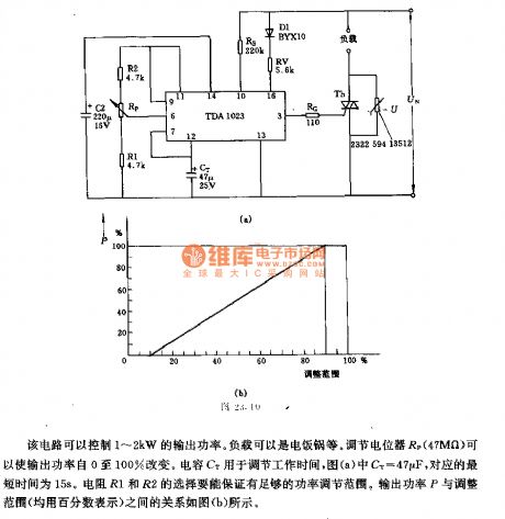
This circuit can control 1~2kW output power. The load can be electric cooker and so on. Adjusting potentiometer Rp (47MΩ) canmake output power change from 0 to 100%. Capacitor Ct isused for adjusting working time, and in diagram (a), cT=47µF, and the corresponding minimum duration is 15s. Resistord R1 and R2 should ensure engough power adjusting range. The relationshipbetween output power P and adjusting range ( all show as percentage) is shown in diagram (b) . (View)
View full Circuit Diagram | Comments | Reading(1116)
The detector amplifier without cooling
Published:2011/11/30 21:35:00 Author:May | Keyword: detector amplifier, without cooling

This circuit is a low-noise amplifier, its input isconnected with ORP10 lndium antimonide detector workingunder room temperature . Four low noise transistors are connected inparallelfor thefirst step in order to match with low noise level photoresistor (30Ω) connected in input end. Effective noise figure is 3dB, voltage gain is 220, bandwidth is above 1MHz.
(View)
View full Circuit Diagram | Comments | Reading(698)
Blown fuse flash circuit
Published:2011/11/30 21:21:00 Author:May | Keyword: Blown fuse, flash

When fuse is unharmed, neon light NE-2 always shines; when fuse is blown, neon light flashes. Flash speed depends on R1 and C1. This circuit flashes 10 times/s ( it depens on numerical value of components in the diagram) .
(View)
View full Circuit Diagram | Comments | Reading(817)
Semiconductor analog switch circuit
Published:2011/12/1 1:33:00 Author:May | Keyword: Semiconductor, analog switch

High noise immunity operational amplifier analog switch
It uses theanalog electronic switching to replace contact switch, and itcan prevent sparkle and radio interference. The diagram is the circuit using junction field effect transistor and operational amplifier and its equivalent machiinery track. When input signal UE ( or UE1, UE2...) has control signal ( high level 10V) , junction field effect transistor is breakover, and it output signal UA ( anti-phase)through operational amplifier. Diagram shows the similar circuit.
(View)
View full Circuit Diagram | Comments | Reading(764)
Sickroom calling device circuit
Published:2011/11/30 21:14:00 Author:May | Keyword: Sickroom calling device

This circuit is composed of two ICs, its features are that it can use a pair of wires toreplace the calling wires in ten rooms. Every room number uses LED as indication, when people press calling switch, corresponding LED displaysroom number, and emits voice.
(View)
View full Circuit Diagram | Comments | Reading(1058)
Audio frequency therapeutic apparatus circuit
Published:2011/11/9 21:07:00 Author:May | Keyword: Audio frequency, therapeutic apparatus
Audio frequency therapeutic apparatus circuit principle is shown in the diagram. It consists of RC oscillator, preamplifier, push-pull power amplifier and the output current indicator, etc. In fact, it is an audio frequency signal generator with high output power.
In the diagram, transistors VT1 and VT2and some resistor-capacitor unit, etc make up wien bridge oscillator with goodwaveform and widelow-frequency adjustable range.The double potentiometer RP1 can adjust oscillator frequency.
Transistors VT3 and VT4 make up the series push-pull amplifier of non output transformer. VT3 and VT4are two transistors with the same polarity, and theyuse series type, and two bases of the transistor areseparately connectedto the collector and emitter of VT2 in order to get oposite phase signal, thereby lt makes VT3 and VT4's bases add to the same amplitude, phase and oposite oscillator signal.
(View)
View full Circuit Diagram | Comments | Reading(1429)
New type nickel-cadmium battery and battery charger
Published:2011/11/10 2:41:00 Author:May | Keyword: New type, nickel-cadmium battery, battery charger

The principle of this circuit is shown in the following diagram. IC1, IC2, IC3 make up voltage comparator. IC4 is square wave pulse generator. The pulse width and frequencyare controlled by IC1. When IC4 outputs positive pulse, BG4 is turned on, constant current IC3 is charging to battery. When IC4 outputs negative pulse, the output is differentiationed by C2. Then itmakes BG1 and BG2 turn on in a short time. It is discharged to battery.
IC1's output is inhigh level afterthepower turningon. The circuit willbe incharging state. If itneeds to discharge, we should touch discharging button AN. It can make IC1 output low level. BG1, BG2are turned on. The battery starts to discharge. Discharge light LED3 is bright. Charging light LED3 is extinguished. When battery discharges to 0.9V, IC1 outputs high level. BG1, BG2are cut off. Discharging is finished. Charging starts.
When battery is charging to 1.42V, IC1's output is changed low level from high, IC2's output is changed high level from low. (View)
View full Circuit Diagram | Comments | Reading(1165)
Farm and sideline products autoregulation drying box circuit
Published:2011/11/23 21:41:00 Author:May | Keyword: autoregulation drying box
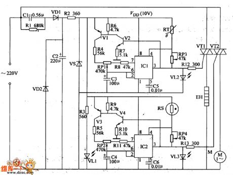
Circuit working principle:
This farm and sideline products autoregulation drying box circuit consists of power source circuit, temperature control circuit and humidity control circuit, is shown in the diagram.
Power source circuit consists of buck capacitor Cl, discharge resistors Rl, rectifier diodes VDl, VD2, filter capacitor C2, current limiting resistors R2, R3, zener diode VS, and power indicator LED VLl.
Temperature control circuit consitsts of thermistance RT ( temperature sensor) , time base intergrated circuit IC1, transistors V1, V2, resistors R4, R6-R8, R12, potentiometers RP1, RP3, capacitors C3, C5, LED VL2, thyristor VT1. At the same time, C3discharges byRP1, R8 and pin 7 of IC1 circuit , when C3 justified voltage decreases to about 3.3V, IC1 pin 3 will output high level to make V1, V2 and VT1 breakover, EH starts heating.
RI and R2 select 1/2W metal film resistors ; R3-R13 use 1/4W metal film resistor or carbon film resistors.RT uses MZ2A positive temperature coefficient thermistor .RS uses ZHC-l or MSO-1 humidity sensitive resistor device . (View)
View full Circuit Diagram | Comments | Reading(1501)
Voltage limiting nickel-cadmium battery charger circuit
Published:2011/11/10 2:37:00 Author:May | Keyword: Voltage limiting , nickel-cadmium battery charger

As shown in diagram 2-16, this charger circuit can charge to four series battery. This circuit also has theautomatic voltage limiting function. VT2 is used for current source. VD5, VD6 and VT2 can stabilize VT2's base voltage at 3V. Meanwhile they are used as charge lights. When the total voltage on the battery closes to the voltage on voltage divider R1, VT1 will start thevoltage limiting function. It is designed according to numeral value of element in the diagram, the currentis 260mAwhen it starts to charge, when Vc reaches to 5V, the current drops to 200mA, when Vc reaches to 6V, the current is almost zero. (View)
View full Circuit Diagram | Comments | Reading(1391)
Nokia 8210 mobile phone travel charger circuit
Published:2011/11/13 20:34:00 Author:May | Keyword: Nokia, mobile phone, travel charger

Nokia 8210 mobile phone travel charger is produced in shanghai, Its crust has label: input AC220V/50Hz (≤30mA), output 4.2V (≤200mA). When it is used in charging, when itneed thecharging Li battery with label 3.6V chaging at 3.98V, the red lamp in the charger circuit is gone out, the green lamp is lit. The whole charging time is about four hours. The author dissects this charger, and draws the circuit diagram. It is referenced by readers when they use or preserve it. Operational amplifier IC in the circuit is used as compartor.
(View)
View full Circuit Diagram | Comments | Reading(2511)
| Pages:385/2234 At 20381382383384385386387388389390391392393394395396397398399400Under 20 |
Circuit Categories
power supply circuit
Amplifier Circuit
Basic Circuit
LED and Light Circuit
Sensor Circuit
Signal Processing
Electrical Equipment Circuit
Control Circuit
Remote Control Circuit
A/D-D/A Converter Circuit
Audio Circuit
Measuring and Test Circuit
Communication Circuit
Computer-Related Circuit
555 Circuit
Automotive Circuit
Repairing Circuit