
Circuit Diagram
Index 1553
Temperature Compensation Circuit
Published:2011/7/11 6:07:00 Author:Robert | Keyword: Temperature, Compensation
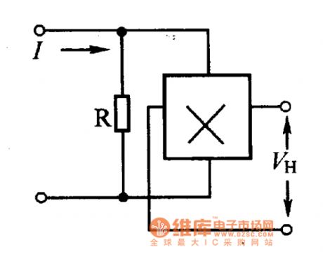
The error caused by the temperature could be compensated by the method of using parallel resistances. Its calculated formula is R=βRin/α.β. The Rin could be found in the parameter table. Its specific circuit is shown in the picture.
The picture shows the temperature compensation circuit. (View)
View full Circuit Diagram | Comments | Reading(503)
Electronic Greetings Card Circuit
Published:2011/7/11 6:00:00 Author:Robert | Keyword: Electronic, Greetings Card

View full Circuit Diagram | Comments | Reading(518)
Electronic Candle Circuit
Published:2011/7/11 6:20:00 Author:Robert | Keyword: Electronic, Candle

View full Circuit Diagram | Comments | Reading(1175)
CX1244S Servo Signal Proecssing Integrated Circuit
Published:2011/7/11 6:28:00 Author:Robert | Keyword: Servo, Signal, Proecssing, Integrated

The CX1244S is a servo signal proecssing IC produced by the Japanese Sony company which is widely used in players.
1.Its functional features.
The CX1244S IC has internal operational amplifier circuit, memory circuit, serial data and clock signal processing circuit, mirror reflection signal processing circuit, tracking error signal processing circuit, focus error signal processing circuit, tracking amplifier gain setting circuit, focus searching voltage and tracking jump voltage and feed voltage control circuit, and other some control and auxiliary function circuits and so on.
2.Its pin's function and data.
The CX1244S IC uses 30-pin dual inline package and its pin's function and data is listed in table 1.
The table 1 shows the CX1244S IC's pin's function and data. (View)
View full Circuit Diagram | Comments | Reading(478)
Single-Chip Radio Integrated Circuit
Published:2011/7/11 6:46:00 Author:Robert | Keyword: Single-Chip, Radio, Integrated


The CXA1238 is a high-integrated AM, FM, stereo decoder single-chip radio IC produced by the Japanese Sony company. It is widely used in many kinds of audio radio systems such as car audio, home audio and so on.
1.Its functional features.
The CXA1238 IC has internal: AM frequency conversion, AM mid-amplifier, wave detection, self-oscillation; FM high-amplifier, FM frequency conversion, FM mid-amplifier, frequency detection and stereo decoding circuit. Its auxiliary circuits have the tuning indication, stereo indication, squelch tuning and other functions.
The CXA1238 IC's main features have the following points:
Low current consumption. When the power voltage is 6V the AM static current is about 8.5mA and FM static current is about 11mA.
Wide application range of the power voltage which means the circuit could work normally at the range of 2-10V.
And so on. (View)
View full Circuit Diagram | Comments | Reading(8967)
Fat Analyzer Principle Circuit
Published:2011/7/11 6:02:00 Author:Robert | Keyword: Fat, Analyzer, Principle

The picture shows the fat analyzer principle circuit. (View)
View full Circuit Diagram | Comments | Reading(512)
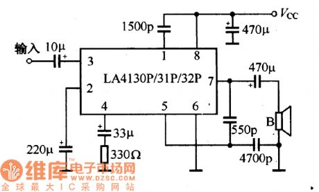
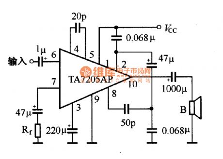
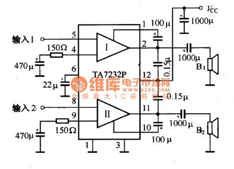
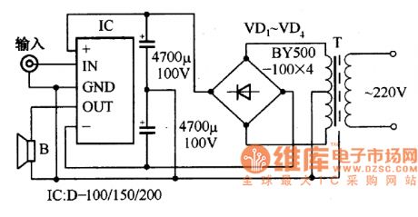
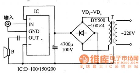
Integrated power amplifer application reference circuit
Published:2011/7/13 10:16:00 Author:Nancy | Keyword: Integrated power amplifer, Application reference circuit
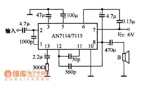
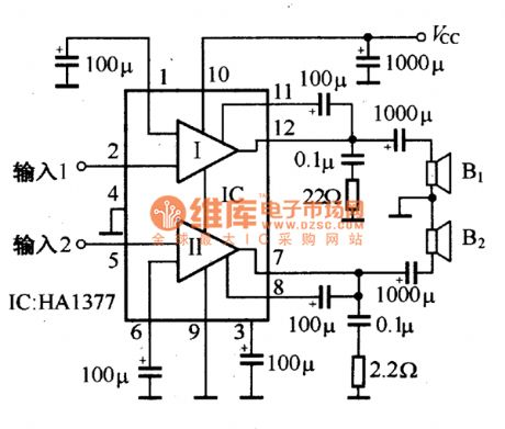
AN-7114/7115 application circuit is shown as above.
LA4130P/31P/32P application circuit is shown as above.
T
A7205AP application circuit
HA1377 application circuit
TA7232P application circuit
Using D series integrated power amplifier can form a mono OTL or OCL audio power amplifier easily, which is shown as the figure. If you use two pieces of D series integrated power amplifier, you can form dual channel power amplifier convenient, which is shown in figure.
single power supply OCL power amplifier circuit
single power supply OTL power amplifier circuit
dual channel OCL power amplifier circuit (View)
View full Circuit Diagram | Comments | Reading(2193)
MYL3 lightning protection zinc oxide varistor appearance circuit
Published:2011/7/13 10:19:00 Author:Nancy | Keyword: lightning protection , zinc oxide varistor

View full Circuit Diagram | Comments | Reading(435)
MYL21 lightning protection zinc oxide varistor appearance circuit
Published:2011/7/13 10:20:00 Author:Nancy | Keyword: lightning protection , zinc oxide varistor

View full Circuit Diagram | Comments | Reading(448)
zero passage comparison circuit
Published:2011/7/13 10:33:00 Author:Nancy | Keyword: zero passage, comparison circuit

The zero passage comparison circuit, inputand outputrelationshipcurve.
The zero passage comparison circuit is shown as figure (a). In an ideal situation, the relationship between input and output is shown in figure (b), UZ stands for the regulated voltage when the diode works in the reverse voltage and UD stands for the voltage drop when the diode works in the forward voltage. The zero passage comparison circuit is often used in the conversion of signal waveform, such as the sine wave coverting into rectangle wave, etc. (View)
View full Circuit Diagram | Comments | Reading(449)
500MHZ Broadband Amplifier Circuit
Published:2011/7/13 6:07:00 Author:Sue | Keyword: Broadband, Amplifier

As seen in the figure is the 500MHZ broadband amplifier circuit. OPA660 can be used to compose direct feedback amplifier with a bandwidth of 500MHz. The input stage consists of OPA660 transconductance amplifier whose gain is decided by feedback resistor R3,R5. Its input stage's voltage gain is G=1+R3/2R5. When the output voltage range is 100mV, the broad width can reach 331MHz; When the output voltage range is 300 mV, the broad width is 362MHz; When the output voltage range is 700mV, the broad width is 520MHz; When the output voltage range is 1.4v, the broad width is 552MHz; When the output voltage range is 2.5v, the brand width is 490 MHz. The circuit uses double 5v as power supply. (View)
View full Circuit Diagram | Comments | Reading(410)
50KHZ Broadband Amplifier Circuit
Published:2011/7/13 6:17:00 Author:Sue | Keyword: Broadband, Amplifier
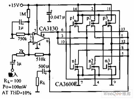
The amplifier with a brand width of 50KHz put CA3600 transistor array paralleling output circuit on the operational amplifier CA3130's output stage. Then the current control ability can improve 2.5 times. The closed-loop gain is 48dB and the brand width is 50KHz. (View)
View full Circuit Diagram | Comments | Reading(840)
555 game timer circuit
Published:2011/6/13 23:24:00 Author:nelly | Keyword: Game, timer
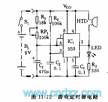
As shown in the figure 11-12, the monostable delay circuit is composed of 555 and R1, RP1, C1, R2, C2. the 2 foot of trigger terminal is connected to the joint point of R2, C2, when it is connected to power supply, the 2 foot has a negative pulse which the level is ground, it can set the circuit, the 3 foot is high level, LED turns on. At the same time, C1 is charged by R1, RP1, when C1's voltage is charged to 2/3 VDD of 6 foot's threshold value level, 555 is reset, the 3 foot is low level, LED turns off, buzzer HTD phonates, it shows that the timing time is reached. The timing time td=1.1(R1+RP1)C1. The td of indicative parameter is adjustable in the range of 10s~60s, it can be previously set according to the needs of game.
(View)
View full Circuit Diagram | Comments | Reading(669)
+5V, 1.6A precision switching power supply circuit
Published:2011/7/12 21:19:00 Author:TaoXi | Keyword: +5V, 1.6A, precision, switching, power supply

The +5V, 1.6A precision switching power supply circuit is as shown in the figure. This circuit increases the photoelectric coupler (CNY75A) and the adjustable precision parallel regulator (TIA31). R3 is the current limiting resistor, R4 and R5 are the sampling resistor. When the Vo changes, the sampling resistor will compare with the 2.5V reference voltage of the TL431, so the electric potential of the K port changes to change the LED's operating current and the luminous intensity of the CNY75, then it adjusts the control port current of WSl57 through the optocoupler, so you can fine-tune the duty cycle to realize the purpose of precision voltage. The CNY75A has also played the electrical isolation effect.
(View)
View full Circuit Diagram | Comments | Reading(5147)
555 storage battery protector circuit with stable voltage charging circuit
Published:2011/6/13 23:24:00 Author:nelly | Keyword: storage battery, protector, stable voltage, charging circuit
As shown in the figure 10-22, the protector circuit is composed of two three-terminal voltage stablizing units and two 555, it includes charge protection and discharge protection. It has the functions of overcharge protection, steady voltage charge, over-discharge protection and short circuit protection.
The charge protection circuit is made of IC1(555)and 7812, 7815 three-terminal regulators. 7812 provides 555 circuit with stable +12V voltage. When it is just charging, the storage battery is charged by J1-1 normally-closed contact. (View)
View full Circuit Diagram | Comments | Reading(828)
555 disconnection photoelectric isolation protecting circuit
Published:2011/6/13 23:25:00 Author:nelly | Keyword: disconnection, photoelectric isolation
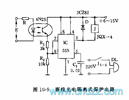
As shown on the figure 10-9, the circuit consists of the CCD and monostable trigger circuit. Gernerally, the CCD 4N25's LED has a current ration. Once it is power-off by some faults, the diode will not light and the 4N25's will be cut off, the 555's 2 foot will be low power level. Then the J will release and the J1-1 will turn off to protect the circuit. This circuit can be used in other occasions, such as distant warning.
(View)
View full Circuit Diagram | Comments | Reading(1418)
+12V, 0.5A single chip switching power supply circuit
Published:2011/7/12 21:27:00 Author:TaoXi | Keyword: +12V, 0.5A, single chip, switching, power supply

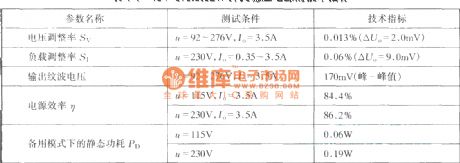
The +12V, 0.5A single chip switching power supply circuit is as shown in the figure. The output power is 6W. When the input AC voltage is in the range of 110~260V, the voltage relative regulation Sv≤1%, when the load current changes greatly, the load relative regulation SI=5%~7%. In order to simplify the circuit, we use the basic feedback mode.
After you connect the power, the 220V AC is bridge type rectified and filted by C1 firstly to get the +300V DC high voltage, then it supplies the operating voltage to WS157 through the primary coil N1 of the high frequency transformer.
(View)
View full Circuit Diagram | Comments | Reading(3901)
100kHz 600W power factor correction circuit
Published:2011/7/12 21:36:00 Author:TaoXi | Keyword: 100kHz, 600W, power factor, correction circuit

The 100kHz 600W power factor correction circuit (PFC) is as shown in the figure, it uses the ZVT--PWM boost topology. In order to reduce the cost, the main switching tube uses the IGBT tube with the TO-220 appearance which is produced by the IR company; the IRGB30U is connected with the 4.4 nF capacitance, and it has the softening switch function and it reduces the turn-off power loss. Although the auxiliary switch has the low RMS current, but it bears the high turn-off current, so we use the MOSFET tube IRFP450(500V, 16A, 150W).
The circuit output voltage is 380V, the input voltage is AC 90~260V. The efficiency of this power correction circuit has relation ship with the operating range of the input voltage. When the ZVT PFC circuit is operating in the 100kHz, and the AC input voltage is in the range of 180~260V, the total efficiency is 97% ~ 98%.
(View)
View full Circuit Diagram | Comments | Reading(3108)
15V/3.5A 52W switching power supply circuit
Published:2011/7/12 21:49:00 Author:TaoXi | Keyword: 15V/3.5A, 52W, switching, power supply circuit

The 15V/3.5A 52W switching power supply circuit which is composed of the MC33374T/TV is as shown in the figure. The permitted range of the AC input voltage u is 92~276V. The rectifier bridges VD1~VD4 use four 1N5406 type 3A/600V siliconrectifier tube. The primary protection circuit is composed of the RC absorbing circuit (R2, C2) and the clamping circuit (VDz, VD5), it can effectively inhibit the peak voltage which is produced the leakage inductance of the high frequency transformer to protect the MC33374 internal power switching tube away from the damage. The VDz uses the P6KE200A type transient voltage suppression diode (TVS), the reverse breakdown voltage UB=200V. The VD5 uses the MURl60 type ultrafast recovery diode (SRD).
(View)
View full Circuit Diagram | Comments | Reading(1416)
400MHZ Differential Amplifier Circuit
Published:2011/7/13 6:31:00 Author:Sue | Keyword: Differential, Amplifier
In the figure, it is the 400MHz differential amplifier. The brandbroad operational transconductance amplifier, the buffer OPA660 can compose differential amplifier with a brand width of 400MHz. The high speed buffer amplifier BUF601 serve as buffer output stage. The circuit gain G=R9/(R8+1/gm). In the formula, gm is OPA660 transconductance's transconductance gain. When R16=650Ω, OPA660's quiescent current is about 10mA and the transconductance is about 0.08A/V(see the figure 1.112). (View)
View full Circuit Diagram | Comments | Reading(355)
| Pages:1553/2234 At 2015411542154315441545154615471548154915501551155215531554155515561557155815591560Under 20 |
Circuit Categories
power supply circuit
Amplifier Circuit
Basic Circuit
LED and Light Circuit
Sensor Circuit
Signal Processing
Electrical Equipment Circuit
Control Circuit
Remote Control Circuit
A/D-D/A Converter Circuit
Audio Circuit
Measuring and Test Circuit
Communication Circuit
Computer-Related Circuit
555 Circuit
Automotive Circuit
Repairing Circuit