
Circuit Diagram
Index 1552
Width modulation, frequency modulation hybrid type switching power supply (2)
Published:2011/7/12 1:34:00 Author:TaoXi | Keyword: Width modulation, frequency modulation, hybrid type, switching, power supply
The control circuit is composed of the VT902~VT904. When the power supply is working, the induced voltage of the transformer T901's sampling windings ⑦~⑧ is rectified by the diode VD911 to supply to the error amplifier for the sampling amplification. The error voltage outputs from the collector electrode to the base electrode of VT903 to control the VT903's bias voltage. And the output pulse of the ⑦ ~ ⑧ end-windings is differentiated by the R919 and C913 to add to the base electrode of VT903. The two signals is superimposed to control the conduction and cut-off of VT902 and VT903. When the two tubes is cut-off, the rectangular pulse voltage of the feedback winding ⑨~⑩ ports is rectified by VD901 to establish the composite voltage on the capacitor C910, so the VD910 is anti-bias cut-off, the VT901 conducts.
(View)
View full Circuit Diagram | Comments | Reading(588)
Capacitive voltage divider type clamping single-ended flyback type switching power supply
Published:2011/7/12 1:47:00 Author:TaoXi | Keyword: Capacitive, voltage divider type, clamping, single-ended, flyback type, switching, power supply
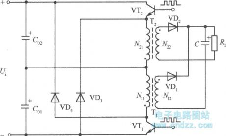
The capacitive voltage divider type clamping single-ended flyback type switching power supply is as shown in the figure. When the VT1 is in the conduction state, the capacitance C02 charges, the COl discharges, the circuit adds the 1/2 input voltage to the original edge winding N1l of the transformer T1; when the VTl is in the cut-off state, the voltage polarity of Nll reverses, when the collector-emitter voltage Ucel of VT1 reaches the input voltage Vi, the diode VD4 conducts, the Ucel is clamped; similarly, when the VT2 is in the conduction state, the C02 discharges, the C0l charges, the circuit adds the 1/2 input voltage to the original edge winding N2l of the transformer T2; when the VT2 is in the cut-off state, the voltage polarity of N2l reverses, after the VD3 is conducted, the Uce2 is clamped by the input voltage Vi.
(View)
View full Circuit Diagram | Comments | Reading(856)
The wSl57 and WSl06
Published:2011/7/12 1:59:00 Author:TaoXi


The appearances and the pin arrangements of the wSl57 and WSl06 are as shown in figure (a) and (b).
Both of them belong to the surface installation component (SMC), they have different package types and pin numbers. In fact the WSl57 only has three pins, it belongs to the three-port component. D is the drain electrode of the MOSFET, the C is the control port, the S is the source electrode. The WSl06 uses the SMD-8 package, it has six S poles, the rest of the poles are the D pole and C pole, so it is still the three-port component. The wSl57 and WSl06 have the same internal circuit. The internal block diagram of the WSl57 is as shown in the figure, it is composed of the l00kHz oscillator, the reference voltage source, the PWM comparator, the control circuit, the driver stage, the power switch tube and the undervoltage, overcurrent and thermal protection circuits.
(View)
View full Circuit Diagram | Comments | Reading(676)
VMOS tube switching power supply (1)
Published:2011/7/12 2:09:00 Author:TaoXi | Keyword: VMOS tube, switching power supply

The stabilized voltage power supply circuit which uses the VMOS tube as the switch device is as shown in the figure. In this figure, the VT5 is the VMOS power transistor, it is the switch adjustment device of this power supply; the L1 is the energy storage inductance; VD3 is the free-wheeling diode, VT3 is the MOSFET which can be used as the constant current source of VTl and VT2 to supply the 1mA constant current for the emitters; Cl is the input filter capacitance; C5, C6 and C7 are the output filter capacitances.
In order to reduce the power consumption of the switching adjustment tube VT5 and improve the flip speed of it, this circuit uses the bootstrap network which is composed of the R5 and C4. When the VT5 is in the cut-off state, the source potential is 0V, the input voltage charges the C4 through the resistor R4 of the diode VD2, so the voltage of C4 closes to the input voltage. (View)
View full Circuit Diagram | Comments | Reading(855)
VMOS tube switching power supply application circuit (3)
Published:2011/7/12 2:33:00 Author:TaoXi | Keyword: VMOS tube, switching, power supply, application circuit

The VMOS tube switching power supply application circuit is as shown in the figure, it is designed as one kind of push-pull switching power supply which uses the TL494 switch integrated circuit component as the control circuit.
In the figure, the TL494 is used as the control circuit of the power supply, in addition to being the oscillation outside source, it is also responsible for the task of adjusting and stabilizing the output voltage. The oscillation frequency is decided by the external components R1 and C1. The switching frequency of this power supply is 100kHz. The VD1 and VD2 are the isolation diodes, the operating voltage is 33V. T is the push-pull output transformer, the primary center tap of it is connected with the DC 12V input power supply. The secondary stage is connected with the output bridge rectifier circuit. The output filter is composed of the current choking coil and the filter capacitance C3.
(View)
View full Circuit Diagram | Comments | Reading(8069)
Practical circuit of the half-bridge type switching voltage stabilization power supply
Published:2011/7/12 3:14:00 Author:TaoXi | Keyword: Practical circuit, half-bridge, switching, voltage stabilization, power supply

The practical circuit of the half-bridge type switching voltage stabilization power supply is as shown in the figure. The half-bridge type converter is composed of the VTl, VT2, T2, C6 and C7. The control signal is amplified by the VT3 and VT4, and it drives the switching tubes VT1, VT2 to alternately turn on and off through the transformer T1. The two ends of the T2's primary coil is connected with the midpoint of C6, C7 and the midpoint of VTl, VT2, so it can couple the power signal to the secondary stage of T2. And it outputs the stable DC through the VDl6, VDl7 full-wave rectification and the L6, C28 two-stage filtering.
The control circuit uses three dual NAND gate ICs as the main part. The JD2 is the timer, it produces the 20kHz square wave. The two monostable triggers are composed of the JD3 and JD4, and the two monostable triggers form the pulse width regulator.
(View)
View full Circuit Diagram | Comments | Reading(599)
Half bridge type converter power supply circuit
Published:2011/7/12 3:42:00 Author:TaoXi | Keyword: Half bridge type, converter, power supply

In the high voltage switch power supply, we usually use the half bridge type converter circuit if the output power is large. The circuit is as shown in the figure. It is composed of two capacitances and two high voltage transistors. When the two transistors are cut-off, if the capacities of the two capacitances are the same and the circuit is symmetrical, the voltage of the capacitance midpoint A is the half of the input voltage. When the VTl is conduction, the capacitance C01 discharges through the VTl and the primary winding N1 of the transformer; at the same time, the capacitance C02 charges through the input power supply, the VTl and the original edge winding N1 of T1. In the process of charging and discharging, the electric potential of midpoint A will reduce exponentially.
(View)
View full Circuit Diagram | Comments | Reading(1493)
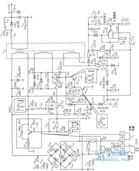
Non-isolated silicon controlled switching power supply
Published:2011/7/12 4:07:00 Author:TaoXi | Keyword: Non-isolated, silicon controlled, switching, power supply

The non-isolated switching power supply which is composed of the silicon controlled is as shown in the figure. The 220V AC voltage adds to the bridge type rectifier which is composed of the VD503, WD505, VD507, VD509 directly. The full-wave voltage that is output by it adds to the cathode of the adjustment device SCR529 through the current choking coil, you can change the output voltage by changing the phase position of the SCR529 trigger pulse. The output voltage is filted by the two-stage RC filter which is composed of the R544, C535 and R545, R546, C536 and it will change into the 155V smooth DC. The VT516 is the error amplifier tube. The VD518 is the zener diode which supplies the reference voltage to the VT516. The sampling voltage divider circuit is composed of the R531, R515, R514.
(View)
View full Circuit Diagram | Comments | Reading(1160)
The practical circuit of the non-isolated switching power supply
Published:2011/7/12 4:27:00 Author:TaoXi | Keyword: practical circuit, non-isolated, switching, power supply

The practical circuit of the non-isolated switching power supply is as shown in the figure, it can be used as the switching power supply of the MuDan TC--483D type color TV set, it is composed of the grid filter which is composed of the C80l, C802, L801; the bridge rectifier circuit which is composed of the VD80l and VD802; the filter which is composed of the R802 and C807, the peak voltage limiter which is assumed by the piezoresistor VD811, the pulse oscillator which is composed of the switch tube VT80l and the pulse transformer T801; the pulse width modulator which is composed of the VT802; the error amplifier which is composed of the VT803.
(View)
View full Circuit Diagram | Comments | Reading(574)
MC33370
Published:2011/7/12 4:45:00 Author:TaoXi

The MC33370 series uses the 8-pin dual-row DIP package (DIP8) or the 5-pin TO (View)
View full Circuit Diagram | Comments | Reading(762)
MOSFET resonance type DC-DC converter circuit
Published:2011/7/12 4:58:00 Author:TaoXi | Keyword: MOSFET, resonance type, DC-DC, converter

The MOSFET resonance type DC-DC converter circuit is as shown in the figure. The Los ella circuit is working through the transformer magnetic saturation and transistor flip overturn. In this circuit, the transformer is operating in the unsaturated mode, it presents the arc-shaped change through the gate feedback voltage of the MOSFET, and it everts the MOSFET by reducing gate voltage.
This AC flows through the transformer primary coil Np. The transformer primary coil and the capacitance C1 produce the reverse-polarity resonance current. The oscillation frequency f of this circuit is decided by the resonant frequencies of the inductance Lp and the capacitor C1 of the transformer primary coil:1/[2π*(Lp*c1)1/2]. (View)
View full Circuit Diagram | Comments | Reading(4338)
The DPCA-Fukang DC7140 image symbol circuit
Published:2011/7/12 0:22:00 Author:Borg | Keyword: DPCA-Fukang, image symbol

Figure: The DPCA-Fukang car circuit diagram1-wire wielding connector; 2-plug connector; 3-connector contactor; 4-connector contactor with marks; 5-fixed connector; 6-fixed connector; 7-wire wielding ground connection; 8-connector ground connection; 9-part shell ground connection; 10-switch (with auto reset); 11-hand switch; 12-converting switch; 13-normally open contactor(auto reset); 14-normally closed contactor (auto reset); 15-hand switch; 16-mechanical switch. (View)
View full Circuit Diagram | Comments | Reading(4934)
IX0689 power supply
Published:2011/7/12 19:29:00 Author:TaoXi | Keyword: power supply

The 300V DC voltage is divided by the R707 and R724, and then this 300V DC voltage adds to the pin-12 of the N701 through the C735 and L701, the pin-12 of the IX0689 is the B port of the internal switching tube, so the switching tube conducts, the current gets in this circuit through the C port of the pin-15, and it gets out through the E port of the pin-13.
The pin-3 and pin-5 of the T701 is the positive feedback winding, when the switching tube is conducting, the pin-5 has the positive polarity and the pin-3 has the negative polarity, the voltage of pin-5 adds to the pin-12 of N701 through the V735, R713 and L701 to increase the current of the switching tube, so this cycle makes the switching tube saturate quickly.
(View)
View full Circuit Diagram | Comments | Reading(1315)
Small power switching power supply circuit produced by the CWl840
Published:2011/7/12 19:34:00 Author:TaoXi | Keyword: Small power, switching, power supply

View full Circuit Diagram | Comments | Reading(661)
CWl525A single-ended common circuit
Published:2011/7/12 19:49:00 Author:TaoXi | Keyword: single-ended, common circuit

View full Circuit Diagram | Comments | Reading(539)
4W backup type switching power supply circuit
Published:2011/7/12 20:04:00 Author:TaoXi | Keyword: 4W, backup type, switching, power supply

The +5V and +12V dual-channel output 4W backup type switching power supply circuit which is composed of the TOP221P is as shown in the figure. This circuit uses one piece of TOP221P(ICl) and one piece of optocoupler PC817A (IC2). The circuit can continue to supply power if the main power is failure, so it can ensure that the data of the CPU and real time clock chip internal RAM will not loss. The input port is connected with the DC voltage Ui. The value of Vi is decided by the change range of the AC input voltage u (such as 85~245V). T is the high frequency transformer, N1 is the primary coil, N2 is the subprime coil, N3 is the feedback coil.
(View)
View full Circuit Diagram | Comments | Reading(1881)
300kHz 600W ZVT--PWM boost converter
Published:2011/7/12 20:55:00 Author:TaoXi | Keyword: 300kHz, 600W, ZVT--PWM, boost converter

The power stage circuit is as shown in the figure, you can design the switching voltage stabilization power supply with the 300kHz switching frequency, 600W output power and 300V output voltage by using the ZVT--PWM boost converter. The input voltage is 150~200V.
The Ls is the saturable reactor, it can be used to eliminate the ringing between the Lr and the VT1 output capacitance, it uses the Toshiba spike killer SAl0×6×4.5 magnetic core, the circle number is five. You can use the rapid recovery diode VD2 to stop the conduction of the VTl ontology diode. If there is no diode, the VTl will conduct the current to supply power to the resonance between the Lr and the VTl output capacitance. So when the VT1 is closing, it will bear the reverse recovery problem.
(View)
View full Circuit Diagram | Comments | Reading(2023)
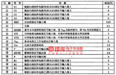
CH91260--the microcomputer dialing integrated circuit
Published:2011/7/13 10:29:00 Author:Borg | Keyword: microcomputer dialing, integrated circuit

CH91260 is the microcomputer dialing integrated circuit,which is widely used in wireless phones.1.function featuresCH91260 contains the dual audio/pulse compatible with dialing circuit, key switch signal encoding/decoding circuits and so on.2.pin functions and dataThe pin functions and data of CH91260 is shown in table 1.
Table 1 pin functions and data of CH91260 (View)
View full Circuit Diagram | Comments | Reading(502)
J8O-1A57-the communication single chip microcomputer integrated circuit
Published:2011/7/13 10:46:00 Author:Borg | Keyword: communication single chip, microcomputer

1.function featuresJ80-1A57 contains the wireless emitting and receiving control circuit, key switch encoding/decoding circuit, charge detection circuit, battery low-voltage circuit, PLL signal process circuit, keypad indicator control circuit, field strength detection circuit, buzzer drive control circuit, 2 lines of clock oscillating circuits, ringing switch control circuit and other indicator drive control circuit, etc.2.pin functions and dataJ80-1A57 is in 44-pin package, whose pin functions and data are listed in table 1-1.
(View)
View full Circuit Diagram | Comments | Reading(546)
CH25610--the pulse/dual audio dialing integrated circuit
Published:2011/7/13 10:55:00 Author:Borg | Keyword: dual audio dialing, integrated circuit
CH25610 is a the pulse/dual audio dialing integrated circuit, which is used in communication dialing control circuits, and it is often used in wire/wireless phones.1.function featuresCH25610 contains pulse/dual audio with dialing, keypad switch signal encoding/decoding and other function circuits.2.pin functions and dataPin functions and data of CH25610 are listed in table 1.
Table 1. Pin functions and data of CH25610 (View)
View full Circuit Diagram | Comments | Reading(571)
| Pages:1552/2234 At 2015411542154315441545154615471548154915501551155215531554155515561557155815591560Under 20 |
Circuit Categories
power supply circuit
Amplifier Circuit
Basic Circuit
LED and Light Circuit
Sensor Circuit
Signal Processing
Electrical Equipment Circuit
Control Circuit
Remote Control Circuit
A/D-D/A Converter Circuit
Audio Circuit
Measuring and Test Circuit
Communication Circuit
Computer-Related Circuit
555 Circuit
Automotive Circuit
Repairing Circuit