
Circuit Diagram
Index 1556
Simple Practical Stable and Reliable 5V to 3.3V Circuit
Published:2011/6/15 10:58:00 Author:Michel | Keyword: Simple, Practical, Stable, Reliable, 5V to 3.3V Circuit


Reducing the power supply voltage can reduce dynamic power consumption thus electronic devices's work voltage drops from 5V to 3.3V even lower value such as 2.5V and 1.8V.Many chips still use 5 V power supply voltage because of kinds of restricting reasons.So in many designs, 5 V logic system and 3.3 V logic system with low voltage coexist.With the introduction of more low voltage standard, different power supply voltage and different logic level device interface problems will exist in a long time, therfore,there is a PWL conversion when devices interface.Level conversion module mainly uses the 74 ALVC164245 devices and it can achieve mutual conversion between 3.3 V voltage and 5 V voltage. (View)
View full Circuit Diagram | Comments | Reading(1544)
Micro Controller MC9S08AW32 and HT1621 Interface Circuit
Published:2011/6/15 8:16:00 Author:Michel | Keyword: Micro Controller, Interface Circuit


Liquid crystal display system hardware interface circuit mainly contains micro controller,MC9S08AW32, liquid crystal display module LCD, backlight,liquid crystal drive chip HT1621,key module and resistance and capacitance components etc. and it is showed as the figure 1.
In the figure 1, PTC0 ~ PTC2 port of micro controller MC9S08AW32 are connected to liquid crystal drive chip HT1621's chip selecting signal port (CS), write signal control port (WR) and data signals port (DATA)respectively and they connect pull-up resistors to high PWL respectively. Read signal control port (RD) only needs to connect to high PWL via pull-up resistors because there is no necessary to use HT1621's Read operation.The MC9S08AW32 PTE0 ~ PTE7 port connects key module, PTC3 port connects NPN transistor, which is to control back panels. (View)
View full Circuit Diagram | Comments | Reading(3182)
General Wireless Alarm Launch and Receiving Circuit
Published:2011/6/15 6:57:00 Author:Michel | Keyword: General Wireless Alarm, Launch, Receiving, Circuit

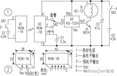
The circuit is showed as the picture and the transmitter is composed of wireless remote control launch module,A1 and battery G1 and the power switch SA1. Receiving alarm consists of wirless remote control receiving module,A2 andsimulated sound integrated circuit A3 etc.
Usually,A1 module built-in antenna launches out into the surrounding space about 250 ~ 300 MHz frequency modulation electromagnetic wave.Within effective distance,the wave is received by tiny receiving antenna inside A2 module.The wave outputs low PWL after its modulatation,amplification,test ,delay and PWL change.A3 does not work because TG PIN's low PWL, acoustic device B has no voice.Once the receiving and launching distance exceeds 15mA2 will be not able to receive enough strong transmitting signal and then A2 low pin changes into high PWL,which tirggers inside circuit work of A3.
(View)
View full Circuit Diagram | Comments | Reading(494)
LM2407T-Video output amplifier circuit
Published:2011/7/10 2:31:00 Author:leo | Keyword: Video, Output amplifier circuit

LM2407T is a type of video output amplifier circuit made by America national semiconductor company and is widely used in computer color screen.
1.Function features:The integrated circuit LM2407T contains three video output amplifier circuits, video output power supplying circuit, and other related circuits with same functions. 2.Pin functions and data:LM2407T adopts 11-pin single line package which you can check more from the picture. Other related data is also shown in the picture. (View)
View full Circuit Diagram | Comments | Reading(697)
IC Synchronous Detection Circuit of 2MHZ Input Signal Srequency
Published:2011/6/14 13:06:00 Author:Michel | Keyword: 2MHZ, Input Signal Srequency, IC, Synchronous Detection Circuit

Circuit's Functions
MC1496 is widely used as IC balance modulation circuit, the basic circuit connection are the same with modulation circuit.But it's output circuit adds level shifting circuit so it can be used in synchronous detection and gets EO =E.COSθ output. Without switch circuit, according to the the element parametersof the circuit , the signal frequency reaches 2 MHZ.Circuit's Work PrincipleMC1496 is composed of double transistor differential circuit and its output is open-collector type, and it needs connect outside load resistor.In order to perform the dc coupling and the differential amplifiers receiving A1 output end signal,OP amplifier A2 forms a 3 times constitutes level shifting circuit. (View)
View full Circuit Diagram | Comments | Reading(2527)
Relaxation Oscillation Circuit of Unijunction Transistor
Published:2011/6/14 13:12:00 Author:Michel | Keyword: Unijunction Transistor, Relaxation Oscillation Circuit
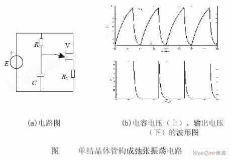
The relaxion oscillating circuit which is composed of uijunction transistor is showed as the picture (a).The initial voltage of capacitor is set to 0.The power supply charges the capacitancevia the resistance R when the power is switched UA of uijunction transistor depends on power voltage E(Ubb) and devices' current-voltage characteristic and peaks and valleys point are also determined by this.Capacitor voltage rises in accordance with the index.Emitter current is small before emitter voltage reaches peak and two ends voltage can be ignored becuase the current that passes through R1 is very small.The uijunction transistor enters negative resistance area and then the diode current flows when the voltgae reaches the peak and UC is equal to UP. (View)
View full Circuit Diagram | Comments | Reading(760)
17W PC Standby Power Supply Circuit of 5V and 3.3 V Output
Published:2011/6/14 13:11:00 Author:Michel | Keyword: 5V , 3.3 V, Standby Power Supply

The picture 3 shows the PC standby circuit which provides both 5V,2A and 3V,2A 's main output.This power supply adds 15V,30mA's auxiliary output with lowest cost.This circuit uses a TOP232Y type singlechip power supply and its total output supply is 17.05W.DC input voltage range is 200~375V. 110V AC 220 / fixed input voltage can be chosen as long as it isconnected to commuting filter and it is unnecessary to add voltage multiplier to commutate 110V AC.This design fully takes TOP232's advantages such as soft start, voltage protection, strictly limited flow characteristics and high switching frequency and its advantages make the high-frequency transformer choose EE19 type chip. (View)
View full Circuit Diagram | Comments | Reading(3314)
LM2437T-The video output amplifier integrated circuit
Published:2011/7/10 2:31:00 Author:leo | Keyword: Video, Output amplifier, Integrated circuit

LM2437T is a kind of video output amplifier integrated circuit made by America national semiconductor company which is widely used in color screen of the computer.
Function feature:The integrated circuit LM2437T contains R, G, B three fundamental color signal amplifier circuit, high voltage power supply circuit, low voltage power supply circuit and other related circuits.
Pin function and data:The integrated circuit LM2437T uses 9 pin single-line package which is widely used in color screen of Samsung 743DFS.The pin function and related data are shown in the picture. (View)
View full Circuit Diagram | Comments | Reading(820)
Quartz Crystal Oscillation Circuit of C-MOS Converter
Published:2011/6/14 13:07:00 Author:Michel | Keyword: C-MOS Converter, Quartz Crystal, Oscillation Circuit
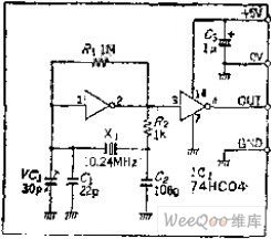
Circuit's Functions Recently,there is a trend that people changes C-MOS for TTL devices.What's more,74HC-series products also got further enrichment.The oscillating circuit composed of C-MOS IC can substitute for clock oscillating circuit composed of level two TTL because TTL IC stops oscillating and causes abnormity easily.However,this circuit is simple with accurate oscillation.
Circuit's Work PrincipleThe partial resistor R1 is connected between input and output ends and make the input end fix on threshold voltage to keep C-MOS changeover job in online linear status. (View)
View full Circuit Diagram | Comments | Reading(608)
Low Frequency FM Circuit of Transistors
Published:2011/7/7 16:18:00 Author:Michel | Keyword: Low Frequency, FM Circuit, Transistors

The picture is low frequency FM circuit of transistors.In this circuit, emitter coupling multivibrator is composed of Vt1 and VT2 and constant current comopsed of VT1 and Vt2 are used between its base and emitter and the base voltage controls the work current.Vt1 and Vt2 can make the VT3's voltage between 0.5~0.6V.If offset voltage is 5 V and the oscillation frequency ≈ 3.3 x1O3 / C1 according to the device parameters and environmental temperature is positive temperature coefficient. VTl is temperature compensation circuit and its purpose diode W knife of base-collector compensates temperature coefficient and at the same time VT1 also can complete level of the shift work of VT4 and VT5 UBE . When the +Ucc-0.6V frequency oscillation signal is taken from the VT3 's collector,it flows through straight capacitance C2 and is added to VT6's base and it outputs frequencysignal from emitter of follower VT6.
(View)
View full Circuit Diagram | Comments | Reading(617)
Temperature Control Circuit of Transistor Temperature Sensor
Published:2011/7/7 15:54:00 Author:Michel | Keyword: Transistor, Temperature Sensor, Temperature Control Circuit
This picture is temperature control circuit of transistor temperature sensor.In this circuit,the voltage and tempreature between the base and emitter is inversely proportional.RP2, R3 ,r4-g9 and it consititute bridge road together.A1 amplifies the unbalanced voltage of the bridge road.A1 outputs 100 mV votlage u when the temperature changes 1 ℃.Please adjust RP2 and when the temperature is 0℃,A1 outputs 0V.Please adjust RP2 and when the temperature is 1℃,A1 outputs 100mV. (View)
View full Circuit Diagram | Comments | Reading(666)
Short Pulse Waveform Generating Circuit of DG201
Published:2011/7/7 15:20:00 Author:Michel | Keyword: Short Pulse, Waveform, Generating Circuit
The picture is a short pulse waveform generating circuit composed of DG201 etc.This circuit is often used for the signal source of measuring sound system transmitting condition or electronic instrument dynamic characteristics.In the circuit,A1's gain is almost 2 and it is used to compensate forthe gain loss of analog switch DG201 and output buffer. When terminal impedance is 600 Ω, circuit's total gain is 1 and it is also used as a buffer meanwhile.
The comparator A2 is used to test positive zero-crossing.It outputs short pulse from sinO° and 74HC74 data latches keeps it synchronous.The output time of the short pulse waveform is provided by outside pulse generator and it is asynchronous with sinusoidal oscillator phase .Thus,on the zero-crossing,74HHC74's Q end outputs high PWL after the short pulse inputing high PWL.It outputs via the buffer composed of VT1~VT4 when the analog switch DG201 conducts. (View)
View full Circuit Diagram | Comments | Reading(460)
Triangle and Square Wave Circuit of LF353
Published:2011/7/7 14:27:00 Author:Michel | Keyword: Triangle, Square, Wave Circuit

The picture is triangle and square wave circuit composed of LF353.The circuit consists of lag comparator A1 and inverse integrator A2,charging and discharging time constant is determinded by (RRP1 + R1) and C1.Now we explain the the oscillation working principle by positive or negative saturated state of A1 when the power supply turns on.
If A1 outputs positive voltage, limiting circuit composed of VD1~VD5 and its voltage +UoH is equal to the voltage of voltage regulator diode and diode forward voltage.Integrators A2 intergrates + UoH voltage and the output voltage U。2 is equal to -UoH/(RRP1+R1)C1(V/s) and A2 output quickly enters saturated state. (View)
View full Circuit Diagram | Comments | Reading(1813)
Pulse Generator Circuit of CA3130
Published:2011/7/7 14:27:00 Author:Michel | Keyword: Pulse Generator, Circuit

This picture is pulse generator circuit composed of CA3130 etc.This circuit uses VD1 and VD2 diode (2 SK30)with high reverse resistance,which makes the charging and discharging time constant adjusted independently.R1, R2, R3 and A1 constitute comparator and S1 connects different capacity capacitors to obtain different period pulse signal. The high and low PWL timeof output waveformcan be set independently and high PWL time is determined by resistance value setting and low PWL time is decided by RP2 resistance value setting.According to the circuit components parameters, and the output pulse cycle is 4 u 5 ~ 1 S. (View)
View full Circuit Diagram | Comments | Reading(1734)
Stable Frequency and Amplitude Sine Wave Output Circuit
Published:2011/6/14 21:19:00 Author:Michel | Keyword: Stable Frequency and Amplitude, Sine Wave, Output Circuit

Circuit's Functions The sine wave oscillation circuit requires that oscillation frequency and output level are very steady.It's hard to realize if common CR oscillation circuit is adopted but this circuit can meet the requirement. square wave can be changed into sine wave when low-pass filter is used.But waveform distortion depends on filter's cutoff characteristics and filter's levels should increase and ultraharmonics are greatly reduced to get low distortion waveform.
Circuit's Work PrincipleThe quartzquartz crystal oscillator circuit generating clocksignal frequency is divided into 1KHZ by frequency division circuit.The waveform dutyfactorrate is set to 50%:50% to reduce thedistortion caused by even-order harmonic .It can use binary counting frequency demultiplier directly.
(View)
View full Circuit Diagram | Comments | Reading(863)
Step Voltage Generating Circuit of Output Fifth Voltage
Published:2011/6/14 13:18:00 Author:Michel | Keyword: Fifth Voltage, Step Voltage, Generating Circuit

Circuit's Functions
Ladder is a waveform that voltage shows ladder shape change with the time increases.In other words,it's a kind of bad slope linear waveform caused by digital circuit.In this circuit,at most 15 steps voltage can be output.The average time of per level is determined by external input clock and level differences of output voltage are equal.This cuircuit can be used if you want to gradually improve the response of the voltage.
Circuit's Work Principle
C1 is four binary counter and it constitutes 4 D - A converter when R - 2R trapezoidal resistor network are added to its output terminal.
(View)
View full Circuit Diagram | Comments | Reading(662)
Stable Up/Stop Phase Short Pulse Waveform Generating Circuit With Synchronous Circuit
Published:2011/6/14 21:15:00 Author:Michel | Keyword: Synchronous Circuit, Stable Up/Stop Phase, Short Pulse Waveform, Generating Circuit

As function generator,oscillator generates short pulse waveform easily.This circuit has not only normal CR oscillator and pulse generator and also contains additional decoder circuit which produces short pulse generator.Short pulse wave mostly is used as the signal source to test audio equipment transfering status or electronic instrument dynamic characteristics.
Circuit's Work Principle
The OP amplifier A1's magnification time is around 2 times and this is to compensate analog switch or output buffer gain loss , and the general magnification timeis1 and it can be used as buffer.
The comparator A2 begans to output burst wave through SIN0 degree and uses IC4 data-latch to make it become synchronous in order to test signal's zero crossing. (View)
View full Circuit Diagram | Comments | Reading(818)
Ultra-low Frequency Sawtooth Wave Generating Circuit of Common Components
Published:2011/6/14 13:16:00 Author:Michel | Keyword: Common Components, Ultra-low Frequency, Sawtooth Wave, Generating Circuit

Circuit's Functions
People immediately associate with OP amp or miller integral circuit composed of discretes when we mention sawtooth wave. But long cycle ultra-low frequency sawtooth wave generating circuit causes linear deterioration because of OP amp input deviation or integral points capacitor insulation resistance.To solve this problem, we can use counter and D - A converter to make the time cycle not be restricted.But, if the output waveform is amplified it will be trapezoidal.Many D - A converter multiples are required to make the wave looks like it is a linearityand the specific multiples depend on application purposes.
(View)
View full Circuit Diagram | Comments | Reading(1121)
Low Distortion and State Variable Two-phase Oscillation Circuit
Published:2011/6/14 13:15:00 Author:Michel | Keyword: Low Distortion, State Variable, Two-phase Oscillation Circuit

Circuit's Functions
The amplifier used in audio equipments needs low distortion signal when it tests.Recently,there are many low distortion OP amplifiers used in audio equipments.If oscillator has distortion, the measurement will be restricted.The state variable circuit has some parts of the active power filter and it can change into oscillators if positive feedback is added.The integrator is composed of two-stage opposite phase amplifier and the high frequency distortion caused by integrator itself reduces 6DB/OCT per stage.This circuit is adopted in low distortion oscillating circuit and if the difference valuefor input and output phase of integrator is 90 degree,it will get 2 phase oscillation output. (View)
View full Circuit Diagram | Comments | Reading(1913)
Basic Circuit of Thermistance Bridge Type Measuring
Published:2011/6/14 21:56:00 Author:Michel | Keyword: Thermistance, Bridge Type, Measuring, Basic Circuit

Basic Circuit of Thermistance Bridge Type Measuring (View)
View full Circuit Diagram | Comments | Reading(532)
| Pages:1556/2234 At 2015411542154315441545154615471548154915501551155215531554155515561557155815591560Under 20 |
Circuit Categories
power supply circuit
Amplifier Circuit
Basic Circuit
LED and Light Circuit
Sensor Circuit
Signal Processing
Electrical Equipment Circuit
Control Circuit
Remote Control Circuit
A/D-D/A Converter Circuit
Audio Circuit
Measuring and Test Circuit
Communication Circuit
Computer-Related Circuit
555 Circuit
Automotive Circuit
Repairing Circuit