
Basic Circuit
Index 74
TinyCAD for schematic drawing
Published:2012/9/19 21:18:00 Author:Ecco | Keyword: TinyCAD, schematic drawing

TinyCAD is a program for drawing circuit diagrams commonly known as schematic drawings. It supports standard and custom symbol libraries. It supports PCB layout programs with several netlist formats and can also produce SPICE simulation netlists.TinyCAD is an open source schematic capture program for MS Windows.Use TinyCAD to produce professional circuit diagrams and export net list information to PCB applications.
Download TinyCAD from Project Home: tinycad.sf.net
Join the tinyCAD user group http://uk.groups.yahoo.com/group/tinycad/
3 Responses to “TinyCAD for schematic drawing”
(View)
View full Circuit Diagram | Comments | Reading(1258)
LDR = Light Dependent Resistor = Photoresistor
Published:2012/9/19 21:14:00 Author:Ecco | Keyword: LDR, Light Dependent Resistor , Photoresistor
You’re asking what is LDR? It stands for Light Dependent Resistor or Photoresistor, which is a passive electronic component, basically a resistor which has a resistance that varies depending of the light intensity. A photoresistor is made of a high resistance semiconductor that absorbs photons and based on the quantity and frequency of the absorbed photons the semiconductor material give bound electrons enough energy to jump into the conduction band. The resulting free electrons conduct electricity resulting in lowering resistance of the photoresistor. The number of electrons is dependent of the photons frequency.
How does the LDR (photoresistor) works
The resistance is very high in darkness, almost high as 1MΩ but when there is light that falls on the LDR, the resistance is falling down to a few KΩ (10-20kΩ @ 10 lux, 2-4kOmega; @ 100 lux) depending on the model.
Light dependent resistors come in different shapes and colors. LDRs are very useful in many electronic circuits, especially in alarms, switching devices, clocks, street lights and more. There are some audio application uses such as audio limiters or compressors. It is used to turn ON or OFF a device according to the ambient light.
On electroschematics.com we have some circuits that uses the photoresistor.They are all tagged as LDR. Here are some of them:
Light alarm circuit with LDRThis musical light alarm circuit is very simple, uses only 7 components, a LDR and a 3.6 V battery or 3 x 1.2 volts rechargeable batteries. The well-known UM66 is used as the sound generator and will give a pleasent wake up alarm.
LDR PC Desk LampMost of the PC desk lamps available in the market light up whenever there is an input power. These don’t take into account whether there is a real need for the light or not. Here is an intelligent PC desk lamp circuit that overcome the problem.
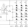
Christmas LED DecorationUsing this simple circuit, you can make an 18 LED flasher to decorate the X’Mas Tree. The White, Blue and Red LEDs flash at different rates to give a colorful display. It is a light sensitive circuit so that it will turn on in the evening automatically and stays on till morning.
Flashing LED with LDR with photoresistorIn this flashing led lights circuit, the LDR or photoresistor is connected in such way that when the light intensity varies it will influence the flashing frequency and the brightness of the LEDs. You can arrange the LEDs D1 to D (View)
View full Circuit Diagram | Comments | Reading(1170)
L14F1, L14F2 Datasheet
Published:2012/9/18 21:37:00 Author:Ecco | Keyword: Datasheet
The L14F1/2 is a silicon photodarlington mounted in a narrow angle, TO-18 package.
L14F1 and L14F2 features
hermetically sealed package
narrow reception angle
One Response to “L14F1, L14F2 Datasheet”
(View)
View full Circuit Diagram | Comments | Reading(594)
LM338 datasheet
Published:2012/9/18 21:37:00 Author:Ecco
The LM138/LM238/LM338 are adjustable 3-terminal positive voltage regulators capable of supplying in excess of 5A over a 1.2V to 32V output range. They are exceptionally easy to use and require only 2 resistors to set the output voltage. Careful circuit design has resulted in outstanding load and line regulation comparable to many commercial power supplies. The LM138 family is supplied in a standard 3-lead transistor package.
LM338 features
GUARANTEED 7A PEAK OUTPUT CURRENT
GUARANTEED 5A OUTPUT CURRENT
ADJUSTABLE OUTPUT DOWN TO 1.2V
LINE REGULATION TYPICALLY 0.005% /V
LOAD REGULATION TYPICALLY 0.1%
GUARANTEED THERMAL REGULATION
CURRENT LIMIT CONSTANT WITH TEMPERATURE
STANDARD 3-LEAD TRANSISTOR PACKAGE
2 Responses to “LM338 datasheet”
(View)
View full Circuit Diagram | Comments | Reading(830)
BC546, BC547, BC548, BC549, BC550 Datasheet
Published:2012/9/18 21:36:00 Author:Ecco | Keyword: Datasheet
BC546, BC547, BC548, BC549, BC550 are NPN switching and amplifier transistors with low noise and working at high voltage.
Pinout configuration (View)
View full Circuit Diagram | Comments | Reading(3206)
TL496 datasheet
Published:2012/9/18 21:36:00 Author:Ecco | Keyword: datasheet
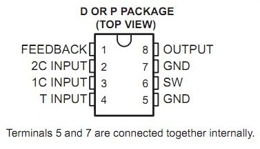
The TL496C power-supply control circuit is designed to provide a 9-V regulated supply from a variety of input sources. Operable from a 1- or 2-cell battery input, the TL496C performs as a switching regulator with the addition of a single inductor and filter capacitor. When ac coupled with a step-down transformer, the TL496C operates as a series regulator to maintain the regulated output voltage and, with the addition of a single catch diode, time shares to recharge the input batteries.The design of the TL496C allows minimal supply current drain during standby operation (125 μA typical). With most battery sources, this allows a constant bias to be maintained on the power supply. This makes power instantly available to the system, thus eliminating power-up sequencing problems.
(View)
View full Circuit Diagram | Comments | Reading(752)
Simple pulse position modulation circuit
Published:2012/9/18 21:36:00 Author:Ecco | Keyword: Simple pulse , position modulation
In pulse position modulation, the amplitude and width of the pulses are kept constant, while the position of each pulse with reference to position of reference pulse, is changed according to the instantaneous sampled value of the modulating signal. Below shown circuit diagram is the simplest pulse position modulation circuit using IC-555.
With this type of circuit, the position of each pulse changes. Both width and period of the pulses vary with the modulating signal. Due to modulating signal at pin 5 ( Control voltage pin ), the UTP level changes to (2Vcc/3)+Vmod.
When Vmod increases, the UTP level increases and hence pulse width also increases. If Vmod decreases, UTP level decreases and pulse width also decreases. Thus the pulse width varies.
The pulse width is given by,
W = – (R1+R2) Cin [ (Vcc-UTP)/(Vcc-0.5UTP) ].
The period is given by,
T = W+0.693R2C
The space between the pulses which is constant is given by 0.693 R2C.This circuit has many application a quick example is, it is used in communication application for transferring voice or data.
One Response to “Simple pulse position modulation circuit”
(View)
View full Circuit Diagram | Comments | Reading(557)
First-order butterworth active low-pass filter
Published:2012/9/18 21:33:00 Author:Ecco | Keyword: First-order butterworth, active, low-pass filter
Butterworth filter is a type of filter whose frequency response is flat over the passband region. Low-pass filter (LPF) provides a constant output from DC up to a cutoff frequency f(H) and rejects all signals above that frequency. Circuit diagram shown below is a first-order low-pass Butterworth filter that uses RC network for filtering. Loading of the RC network is avoided by using the Op-Amp which is configured for non-inverting mode. Resistors R1 and Rf determine the gain of the filter.
Op-Amp ( 5 terminal )
3 Resistors
1 Capacitor
Voltage sources
Af = 1+Rf/R1
f (H) = 1/(2πRC)
In the above circuit the component XSC1 is the Oscilloscope which is used to verify the circuit so don’t get confused with it. In the above circuit the cutoff frequency is decided the resistor R and capacitor C. You can choose any desired value to fix the cutoff frequency. In the above circuit i choose the cutoff frequency to be approximately 5KHz so i used the resistor R of value 10KΩ and capacitor of value 3nF. You can change it if you want to by using the above cutoff frequency formula.
The first order low-pass filter has a practical slope of -20 dB/decade. The low-pass filter has a constant gain Af from 0 to high cutoff frequency f (H). At f(H) the gain is 0.707Af and after f (H) it decreases at a constant rate of 20 dB/decade. The frequency f = f (H) is called the high cutoff frequency because the gain of the filter at this frequency is down by 3 dB ( =20log(10) 0.707 ) from 0 Hz.
The AC analysis of the above circuit is given below. But it is not exactly for the above circuit. The cutoff frequency is now made 20kHz. For getting cutoff frequency 20kHz you need resistor of value 1KΩ and capacitor of value 7.96nF.
If you have any doubt in the circuit please let us know by comments.
2 Responses to “First-order butterworth active low-pass filter”
(View)
View full Circuit Diagram | Comments | Reading(800)
Precision full wave rectifier circuit
Published:2012/9/18 21:31:00 Author:Ecco | Keyword: full wave rectifier
The use of Operational amplifiers can improve the?performance?of a wide?variety?of signal processing circuits. In rectifier circuits, the voltage drop that occurs with an ordinary semiconductor rectifier can be eliminated to give precision rectification.The below shown circuit is the precision full wave rectifier. It consists of following sections:
The input voltage Vin is applied to one terminal of the summing amplifier along with resistor R3 and to the input of the precision rectifier. The output of precision rectifier is applied to another terminal of summing amplifier. The precision half-wave rectifier circuit uses an inverting amplifier configuration.
When the input signal Vin is positive, Op-Amp output terminal is negative, Diode D1 is reverse biased and D2 Diode is forward biased, the circuit is
Vb = -(R2/R1) * Vin
In the circuit, R1 and R2 have been chosen such that R2 = 2R1.So the voltage at Vb = -2Vin.
Thus during the positive half cycle of the rectified voltage Vb is applied to terminal B of the inverting summing amplifier is -2Vin.
The voltage at terminal A is Va = +Vin. The output from the summing circuit with R3=R4=R5 is Vo = – (Va+Vb). Hence Vo = -(Vin – 2Vin) = +Vin. So during the negative half cycle of the input, the Op-Amp output terminal goes positive, causing D2 to be reverse biased. Without D1 in the circuit, the Op-Amp output would be saturated in the positive direction. However, the positive voltage at the Op-Amp output forward biases the D1. This tends to pull the Op-Amp inverting terminal in a positive direction. But, such a move would cause the Op-Amp output to go negative. So, the output settles at the voltage close to ground level. So to be clear, the negative half-cycle is clipped off. That is Vb=0 and Va = -Vin. Totally the Vo will be ?Vo = -(-Vin+0) = +Vin.
It is seen that the output is a full wave rectified version of the input voltage. A Precision full-wave rectifier is also known as absolute value circuit. This means the circuit output is the absolute value of the input voltage regardless of polarity.
If you any doubt about the circuit please drop it in comments we will respond you.;2 Responses to “Precision full wave rectifier circuit”
(View)
View full Circuit Diagram | Comments | Reading(0)
LA4440 datasheet
Published:2012/9/18 21:30:00 Author:Ecco | Keyword: datasheet
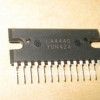
LA4440 is a 2 channel power amplifier that can deliver up to 6W per channel of 19W in bridge connection. It requires minimum number of external parts, it has small pop noise at the time of power supply ON/OFF. It has good ripple rejection of 46dB, small residual noise, built in over voltage and surge voltage protection etc. ideal feature of the IC is its pin-to-pin protection.LA4440 Features
Good ripple rejection : 46dB (typ.)
Good channel separation.
Small residual noise (Rg=0).
Low distortion over a wide range from low frequencies to high frequencies.
Easy to design radiator fin.
Built-in audio muting function.
Built-in protectors.
Thermal protector
Overvoltage, surge voltage protector
Pin-to-pin short protector (View)
View full Circuit Diagram | Comments | Reading(810)
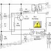
Light activated switch
Published:2012/9/18 21:22:00 Author:Ecco | Keyword: Light activated switch
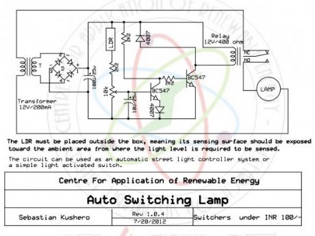
The circuit can be used for switching OFF a particular lamp or group of lamps in response to the varying ambient light levels. The unit once built can be used for switching OFF a lamp when dawn breaks and switching it ON when dusk sets in.
The power supply is a standard transformer, bridge, capacitor network, which supplies a clean DC to the circuit for executing the proposed actions.
Automatic light activated switch circuit schematic
The LDR must be placed outside the box, meaning its sensing surface should be exposed toward the ambient area from where the light level is required to be sensed. The circuit can be used as an automatic street light controller system or a simple light activated switch.
24 Responses to “Light activated switch”
(View)
View full Circuit Diagram | Comments | Reading(722)
Photocoupling zero-crossing control socket circuit using TWH9205
Published:2012/9/18 2:34:00 Author:Ecco | Keyword: Photocoupling , zero-crossing control , socket
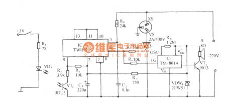
As shown in Figure, the circuit consists of zero-crossing driving switch, photoelectric coupling input circuit, the thyristor control circuit and sound circuit. The phototransistor switching circuit in FIG is connected to the inverting input terminal ( 9 feet) of the differential switching amplifier TWH9205, when the terminal voltage is lower than the clamping voltage of the positive-phase input terminal, i.e., when the phototube 3DU5 is irradiated by light, only when AC os over zero, TWH9205 outputs high to drive SCR VS conduction, then socket XS gets electric, and the electrical equipments connected to XS operate. VS can use 1 ~ 500A triac according to the size of the electrical load power.
(View)
View full Circuit Diagram | Comments | Reading(1196)
Single-phase motor two-speed circuit with auxiliary winding connecting to tap directly
Published:2012/9/18 2:16:00 Author:Ecco | Keyword: Single-phase motor , two-speed circuit, auxiliary winding , tap

As shown in the figure, the circuit uses stator on the auxiliary winding LA to directly connect totap forspeed adjusting, and it has no governor winding.
(View)
View full Circuit Diagram | Comments | Reading(2792)
The AC contactor saving and silent running circuit 1
Published:2012/9/18 1:36:00 Author:Ecco | Keyword: AC contactor, saving , silent running
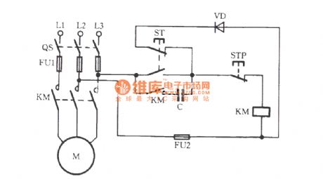
In the circuit shown in figure, when the motor is starting, pressing the start button ST, AC contactor KM will pull in, then the KM auxiliary contacts are closed; releasing the ST, ST normally closed contact will restore the closed state, then the diode VD and KM coils are connected in parallel, and KM self-locking contact connects to the power supply through a capacitor C, KM turns to DC operation. Capacitor C plays buck role in the circuit and makes the AC are flows from top to bottom of coil in the positive and negative half-wave, and it changes AC contactor to DC operation. DC operating noise is minimal, so it is also called AC contactor silent running.
(View)
View full Circuit Diagram | Comments | Reading(982)
Bedside lamp safety switch circuit (2)
Published:2012/9/18 1:50:00 Author:Ecco | Keyword: Bedside lamp, safety switch

Thebedside lamp safety switch shown in the figure uses Triac. RL should use photoresistor with light resistance beingless than 2kΩ.
(View)
View full Circuit Diagram | Comments | Reading(1188)
DC / DC converter circuit diagram using six inverter
Published:2012/9/18 2:28:00 Author:Ecco | Keyword: DC / DC converter , six inverter
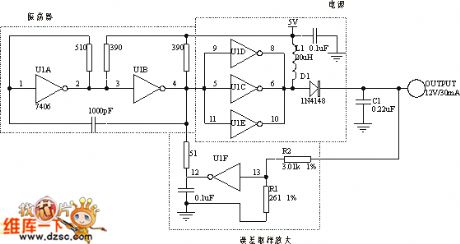
The circuit can be used to adjust voltage by TTL switch threshold. U1A and U1B form the oscillator, and its switching frequencies < 1MHz. The output of the oscillator can drive the three parallel inverters U1C, U1D U1E to provide a higher output current and output power. Its internal output transistor, L1 and D1 form a standard boost converter, when its output is low, the current only flows through the inductor L1; when the output becomes high, the energy stored in the inductor makes anode of D1 become high, D1 conduction charges for C1. The circuit and load characteristics are better than 1%, and output voltage only changes 7% in range of 0 ℃ ~ 50 ℃.
(View)
View full Circuit Diagram | Comments | Reading(939)
L5991 shutdown function achieving circuit diagram
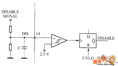
Published:2012/9/18 2:00:00 Author:Ecco | Keyword: shutdown function achieving
L5991's shutdown function is achieved by pin 14. When the voltage on the pin exceeds 2.5 V, the chip will be turned off, only VCC is pulled up to the UVLO threshold, the ffEF will has new start. The chip external force shutdown function can be achieved by the pin, and the circuit is shown in the figure. You can also use the pin to achieve overvoltage protection. In order to avoid the malfunction of this pin caused by noise spikes, in the actual using process, the circuit should bypass connect a thin film capacitor.
(View)
View full Circuit Diagram | Comments | Reading(777)
MAX1458 bridge excitation circuit diagram
Published:2012/9/18 2:21:00 Author:Ecco | Keyword: bridge excitation
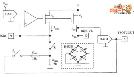
The bridge excitation circuit with digital pressure signal conditioner MAX1458 is shown as the figure. It uses DAC3 output to change the size of the sensor excitation current IBR and realize full-scale calibration. IISRC is the reference current set by RISRC and 9 feet voltage. V1 and V2 form a mirror current source, when the current gain is 14 times, the excitation current IBR = 14IISRC. The IBR programming range is 0.1 ~ 2mA. The on-off state of analog switches S1, S2 is governed by the configuration register. Obviously, when the full-scale output voltage changes, DAC3 will compensate bridge output voltage by BR changing, thereby correcting the errors of the full scale. DAC4 is used to correct the error of full scale temperature coefficient.
(View)
View full Circuit Diagram | Comments | Reading(740)
Dual Precision Monostable Logic circuit (CD4538BC)
Published:2012/9/17 21:41:00 Author:Ecco | Keyword: Dual, Precision Monostable , Logic circuit
The logic diagram of the CD4538BC Dual Precision Monostable is shown in the following schematic diagram. This IC such a dual, precision monostable multivibrator with independent trigger and controls, according to the datasheet. This CD4538BC IC features wide supply voltage range, wide pulse-width range, low standby current, high noise immunity and more. (View)
View full Circuit Diagram | Comments | Reading(630)
Notching filter circuit with variable Q
Published:2012/9/13 22:49:00 Author:Ecco | Keyword: Notching filter , variable Q

A notch filter circuit with a variable quality factorThe notch filter circuit uses two LM110 or SN72310 operational amplifiers as voltage follower, and the circuit is shown in figure.
(View)
View full Circuit Diagram | Comments | Reading(1095)
| Pages:74/471 At 206162636465666768697071727374757677787980Under 20 |
Circuit Categories
power supply circuit
Amplifier Circuit
Basic Circuit
LED and Light Circuit
Sensor Circuit
Signal Processing
Electrical Equipment Circuit
Control Circuit
Remote Control Circuit
A/D-D/A Converter Circuit
Audio Circuit
Measuring and Test Circuit
Communication Circuit
Computer-Related Circuit
555 Circuit
Automotive Circuit
Repairing Circuit