
Basic Circuit
Index 71
FM antenna booster circuit
Published:2012/10/11 2:21:00 Author:muriel | Keyword: FM, antenna booster

This is a low cost fm antenna booster that can be used to listen to programmes from distant FM stations clearly. The antenna fm booster circuit comprises a common-emitter tuned RF preamplifier wired around VHF/UHF transistor 2SC2570 (C2570).Assemble the circuit on a good-quality PCB (preferably, glass-epoxy). Adjust input/output trimmers (VC1/VC2) for maximum gain.
Input coil L1 consists of four turns of 20SWG enamelled copper wire (slightly space wound) over 5mm diameter former. It is tapped at the first turn from ground lead side. Coil L2 is similar to L1, but has only three turns. Pin configuration of transistor 2SC2570 is shown in the fm antenna booster schematic.
FM antenna booster circuit diagram
(View)
View full Circuit Diagram | Comments | Reading(1636)
Ultrasonic pest repellent circuit
Published:2012/10/10 1:59:00 Author:muriel | Keyword: Ultrasonic, pest repellent

There are many ultrasonic pest repellent devices available on the market but a major drawback is that their power output is low and their effectiveness suffers. This electronic pest repellent generates powerful ultrasonic signals to repel pests.In addition to the ultrasonic frequency oscillator built with CD4047, separate push-pull power amplifier (with 2N3055 or TIP31C) and transformer are used to boost ultrasonic signals. The output of the power amplifier is coupled to a tweeter through output transformer X1, which is wound over ferrite core (UU or CC core).
Primary winding consists of 150 turns of 20 SWG while the secondary winding is 40 turns of 24 SWG wire. Adjust potentiometer VR1 for maximum effectiveness.This circuit has not been tested.
Caution! This is a powerful sonic pest repellent circuit so use it only in outdoor places. Do not use this ultrasonic pest repeller near babies or animal pets.
Pest repellent circuit diagram
(View)
View full Circuit Diagram | Comments | Reading(2210)
High Frequency Generator circuit
Published:2012/10/10 1:57:00 Author:muriel | Keyword: High Frequency, Generator

High frequency waveform generator is very useful in electronic experiment and design. This circuit generate sine wave oscillation, but actually we can modify the circuit to generate triangle or square wave function.The core of this waveform generator is MAX038. This integrated circuit chip gives complete function to build a waveform generator/function generator.
High frequency waveform generator circuit diagram
The circuit can be used to generate square wave, triangle, or sine wave by programming the pin inputs (A0:pin 3, A1:pin 4).
A0 A1 WAVEFORM
X 1 Sine wave
0 0 Square wave
1 0 Triangle wave
The frequency can be controlled using current. If we disconnect the 20k RIN from REF (pin 1) and connect it to a DAC, then we can control the frequency using microcontroller or digital interface. We can even control the chip using a quartz crystal (PLL) by controlling the current using a phase comparator output that compares the sync output (pin 14 of MAX038) and a reference clock from quartz crystal oscillator.
This waveform generator integrated circuit chip is very interesting since it can generate 0.1Hz to 20MHz, very wide operating frequency, as expected for every waveform generator instruments. (View)
View full Circuit Diagram | Comments | Reading(1875)
Dynamic compressor – passive components, no power supply
Published:2012/10/10 1:50:00 Author:muriel | Keyword: Dynamic compressor

This dynamic compressor with passive components reduces high signal to a lower, more constant signal. If you look at this compressor schematic , you’ll notice it has no power supply, the required power is obtain thru the output signal.If you respect the schematic values this audio compressor will output a constant 70mV when the input voltage is between 100mV and 10V !
Passive compresor circuit diagram
(View)
View full Circuit Diagram | Comments | Reading(1329)
Electronic Mail Box circuit
Published:2012/10/10 1:47:00 Author:muriel | Keyword: Electronic Mail Box

This Electronic Mail Box circuit generates music intimating the arrival of mail……..The circuit uses a high bright White LED and an LDR to detect the arrival of mail in the box. IC NE 555 is designed as a Schmitt trigger by shorting its trigger pin 2 and threshold pin 6. When the light from the LED illuminates the face of LDR, it conducts taking the pin 6 of IC low. Output pin 3 then remains low inhibiting the buzzer.When a mail falls between the LED and LDR, light from LED will be blocked and the LDR becomes non conducting. This makes the threshold pin of IC high and its output goes high. The high output makes buzzer active and music will be heard. The music stops only when the letter is removed from the box. Keep LED and LDR at the opposite sides of the box. (View)
View full Circuit Diagram | Comments | Reading(1288)
Monostable circuit using TcA965
Published:2012/10/9 22:06:00 Author:Ecco | Keyword: Monostable circuit

The integrated circuit TCA965's reference level U5 is provided by pin 8. If the input signal UE = U6 is less than U5 = U8, the output terminal pin 14 is in low level, and pin 2 is high ; if UE = U6 is high, then the corresponding U8 is decreased, the circuit makes the output flip. Figure b shows the input and output signal waveforms when output time is less( left) and greater (right ) than the monostable time constant. In the latter case, as long as UE = of U6 < U5, the output is immediately restored to low level.
(View)
View full Circuit Diagram | Comments | Reading(1335)
Quick Schmitt trigger circuit
Published:2012/10/9 21:55:00 Author:Ecco | Keyword: Quick, Schmitt, trigger

Adjustment potentiometer RP in circuit can adjust T1 emitter follower so as to change the base level of T2, so the trigger level can be adjusted continuously. In the switching process, 0.6VSS control signal on diode ITT777 is applied to the T3 base. The T2 collector potential is added to the T3 base by regulator ZP. This direct coupling way can eliminate the impact of the RC link.
(View)
View full Circuit Diagram | Comments | Reading(1078)
The Art of Zener Regulation
Published:2012/10/9 2:42:00 Author:muriel | Keyword: Zener

To get precise voltage to a circuit, the simplest and easy way is to use a Zener diode.It uses the reverse breakdown voltage characteristics to maintain a fixed voltage across it The Art of Zener Regulation
D.Mohan kumar
Zener diode ZD is used to generate a regulated DC output. A Zener diode is designed to operate in the reverse breakdown region. If a silicon diode is reverse biased, a point reached where its reverse current suddenly increases. The voltage at which this occurs is known as “Avalanche or Zener “value of the diode. Zener diodes are specially made to exploit the avalanche effect for use in ‘Reference voltage ‘regulators. A zener diode can be used to generate a fixed voltage by passing a limited current through it using the series resistor. The zener output voltage is not seriously affected by the resistor and the output remains as a stable reference voltage. But the limiting resistor is important, without which the zener diode will be destroyed. Even if the supply voltage varies, the series resistor will take up any excess voltage. The value of the series resistor can be calculated using the formula
R = Vin – Vz / Iz
Where Vin is the input voltage, Vz output voltage and Iz current through the zenerIn most circuits, Iz is kept as low as 5mA. If the supply voltage is 18V, the voltage that is to be dropped across R1 to get 12V output is 6volts. If the maximum zener current allowed is 100 mA, then R1 will pass the maximum desired output current plus 5 mA. So the value of R1 appears as
R1 = 18 – 12 / 105 mA = 6 / 105 x 1000 = 57 Ohms
Power dissipation
Power rating of the Zener is also an important factor to be considered while selecting the Zener diode. According to the formula P = IV. P is the power in watts, I current in Amps and V, the voltage. So the maximum power dissipation that can be allowed in a Zener is the Zener voltage multiplied by the current flowing through it. For example, if a 12V Zener passes 12 V DC and 100 mA current, its power dissipation will be 1.2 Watts. So a Zener diode rated 1.3W should be used.
As a rule of thumb, a minimum of 10% of the total current should flow the zener leaving the rest available to the load. By increasing the value of the series resistor, it is easy to reduce the current flowing through the zener but allow a minimum of 5 to 10 mA current through the zener. Then only it will reach the avalanche state to give output voltage.
(View)
View full Circuit Diagram | Comments | Reading(845)
The dynamic driving interface circuit between SAA1064 serial I2C bus and LED display IC
Published:2012/10/8 22:06:00 Author:Ecco | Keyword: dynamic driving, interface circuit, serial I2C bus , LED display IC

Due to the SAA1064's dynamic scanning display depends on the the multiplexer swicthing data latch and time control circuit, the master does not have to intervene, and the dynamic work can best play SAA1064 function, so it is the most common working way. LED -bit numbers in figure and selected data sequence in data manipulation format are corresponding. CEXT is the clock oscillation capacitor which guarantees to work signal for dynamic driving. MX1, MX2 are the common electrode driving signal output terminals of monitor. When it is dynamic scanning, MX1 , MX2 's timing waveforms are shown in Figure as below.
(View)
View full Circuit Diagram | Comments | Reading(1842)
The application circuit of dual-axis magnetic field sensor (integrated magnetic sensor HMC1002) with S / R circuit and serial interface
Published:2012/10/8 22:50:00 Author:Ecco | Keyword: application circuit, dual-axis, magnetic field , sensor , integrated magnetic sensor, S / R circuit , serial interface

It can use a dual - axis magnetic field sensor HMC1002 and two AMP04 draws ( A1, A2 ) to simultaneously measure the magnetic field with X - axis direction and the Y-axis direction. The HMC1002 outputs two ways of voltage signals which are respectively amplified by A1 and A2, then they are input to the analog input terminal and reference terminal 12 of A / D converter TLC2543 and connected to interface circuit μP. The MAX662A is high-efficiency DC / DC converter which can raise +5 V power supply to +10 V to drive IRF7105. The driver's input signal is from μP, and it outputs pulse current to S / R + terminal ( pin 16 ) of HMC1002. C3 shown in figure should be used tantalum capacitor.
(View)
View full Circuit Diagram | Comments | Reading(1307)
The counter composed of digital circuit
Published:2012/10/7 21:58:00 Author:Ecco | Keyword: counter , digital circuit


The counter with digital circuit is shown in the figure, and it uses infrared as detection signals, and it can be used for active target scan counting appliances. It is applied to the production line to rapidly and accurately count move items on the conveyor belt. It also can be used for other purposes such as inbound or outbound passenger counting. The characteristics of the circuit is simple structure, easy making, economical and practical use. The most outstanding advantage is that it can accurately count any items with different shade numbers.
(View)
View full Circuit Diagram | Comments | Reading(1091)
The grating circuit using transistor circuit
Published:2012/10/7 21:50:00 Author:Ecco | Keyword: grating, transistor

When the light on photosensitive element is interrupted, the circuit's relay operates. The photosensitive element and 100kΩ resistor form a voltage divider, thereby controlling the transistor base potential. When light is exposured to it, it is in a low-resistance state, the transistor base potential is very small. Conversely, when the light is blocked, the potential is increased, thereby causing the Schmitt trigger flip, the output stage power transistor is turned on, then relay operates.
(View)
View full Circuit Diagram | Comments | Reading(874)
High voltage regulator circuit with optocoupler
Published:2012/9/28 22:37:00 Author:Ecco | Keyword: High voltage, regulator, optocoupler

The circuit is shown as the figure. Usually, the drive tube needs to use transistor (Figure 9013) with higher withstand. When the output voltage increases, VT55's bias increased, then the forward current of light emitting diode in B5 increases, so that the voltage across poles of photodiodes decreases, the adjustment tube BE junction bias voltage is lowered while the internal resistance increases, so that the output voltage is reduce ; Conversely, the output voltage increases, thereby maintaining the stability of the output voltage.
(View)
View full Circuit Diagram | Comments | Reading(3067)
The typical application circuit of LB140 5-bit LED level indicator driver IC
Published:2012/9/28 22:52:00 Author:Ecco | Keyword: typical application , 5-bit , LED level , indicator, driver IC

BL1405 is widely used in the recorder and tape recorders for level indication.
(View)
View full Circuit Diagram | Comments | Reading(2484)
The interface circuit composed of optocoupler
Published:2012/9/28 22:28:00 Author:Ecco | Keyword: interface , optocoupler

As shown in figure, the optocoupler 4N25 in circuit plays the role of the the coupled pulse signal and isolation microcontroller 89C51 system and output section, so that the current of two parts is independent from each other. Output portion of the ground wire is connected to the chassis or earth, while the 89C51 system power ground wire is floating, and it is not connected to the ground wire of AC power to avoid the effect from power changes of output on microcontroller power, so it reduces interference the system suffered and increase system reliability.
(View)
View full Circuit Diagram | Comments | Reading(2331)
The application circuit of bridge sensor signal conditioner 1B32 macthed with multi-channel pressure sensor
Published:2012/9/28 21:58:00 Author:Ecco | Keyword: application , bridge sensor ignal conditioner , multi-channel pressure sensor

The excitation power can drive multiple bridge sensors after passing AD542 and TIP32. AD542 is the operational amplifier which uses Bi-FET as input stage for the starting buffer. TIP31 is the epitaxial NPN power transistor, and its maximum reverse voltage is 45V, and the maximum collector current is 3A, the maximum power consumption is 40W. The circuit can provide +10 V, 300mA excitation source in the temperature range of -25 ~ +80 ℃. When 1B32's 333.3 GAIN is grounded, the gain is set to 333.3 times.
(View)
View full Circuit Diagram | Comments | Reading(1469)
Precision Monostable circuit
Published:2012/9/28 20:51:00 Author:muriel | Keyword: Precision, Monostable circuit
Here is a Monostable Multivibrator using IC CD4538. It is a Precision Monostable / Astable Multivibrator IC free from false triggering. This can be used for various application in which precise timing cycle is requiredCD 4538 is the Precision Monostable /Astable Multivibrator IC that is free from False triggering. It is more reliable than the popular timer IC 555. Here the IC is wired as a short duration monostable timer using R1 and C1 as timing components. With the given values, output of IC1 remains low for three minutes. By changing the value of C1 or R1 various time intervals can be obtained.
Unlike 555 IC in the monostable mode, here in CD4530, output of IC becomes high at power on and becomes low when the trigger pin5 gets a low-to-high transition pulse. When S1 is pressed, the high going pulse triggers IC and its output goes low. This drives the load through the PNP transistor T1.Load can be an LED, Buzzer etc.
Precision Monostable Circuit diagram
CD4538 Pin connection
(View)
View full Circuit Diagram | Comments | Reading(791)
Power-saving voltage regulator circuit
Published:2012/9/27 22:23:00 Author:Ecco | Keyword: Power-saving, voltage regulator
The regulator have the funtions of general delay regulator, and its main features are: ( 1) When mains voltage is in 220V ± 10 % safe voltage range, the regulator automatically disconnected from the mains, then the mains is added to the load to eliminate its loss. ( 2) When the mains exceeds safe voltage range, it will be automatic step-up or step-down. ( 3) When the load is zero, the regulator is automatically disconnected from the mains to eliminate the no-load loss. ( 4 ) When input voltage is 160V ~ 270V, output voltage is 220V ± 10% to meet national standards. Power is 2500W.
(View)
View full Circuit Diagram | Comments | Reading(1586)
The switching circuit 1 with self-locking ( self-maintaining ) function
Published:2012/9/27 21:55:00 Author:Ecco | Keyword: switching , self-locking , self-maintaining function
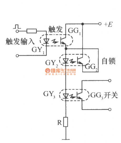
The 3 optical couplers in Figure respectively play the role of the trigger, self-locking and switching. When a start trigger signal is applied to the GY , GG1 gets conduction, then there is current flowing through GY2 and GY3 to turn on GG2 and OG3. When the trigger signal disappears, GY1 does not emit light, then GG1 is cutoff, but at this time, the GG2 has been turned on, and the current of GY2 and GY3 is provided by GG2 passage, GG3 continues to maintain the conductive state, it is equivalent that the switch is still turned on until the power supply voltage E disappears in order to make the circuit restitution.
(View)
View full Circuit Diagram | Comments | Reading(742)
Four gratings circuits using integrated circuit
Published:2012/9/27 21:40:00 Author:Ecco | Keyword: Four , gratings , integrated circuit
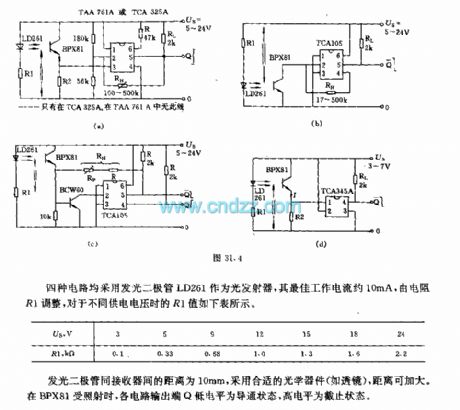
The four circuits use light - emitting diode LD261 as light emitter, and its optimum operating current is about 10mA, and it is adjusted by the resistor R1, the R1 values for the different supply voltages are shown in following table. The distance between the light emitting diode and receiver is 10mm, it uses a suitable optical device ( such as lens ) to increase the distance. When BPX81 is irradiated, each circuit is in turn-on state when output terminal Q is low and off-state when output terminal Q is high.
(View)
View full Circuit Diagram | Comments | Reading(1258)
| Pages:71/471 At 206162636465666768697071727374757677787980Under 20 |
Circuit Categories
power supply circuit
Amplifier Circuit
Basic Circuit
LED and Light Circuit
Sensor Circuit
Signal Processing
Electrical Equipment Circuit
Control Circuit
Remote Control Circuit
A/D-D/A Converter Circuit
Audio Circuit
Measuring and Test Circuit
Communication Circuit
Computer-Related Circuit
555 Circuit
Automotive Circuit
Repairing Circuit