
Basic Circuit
Index 64
30A dual channel schematic diagram
Published:2012/12/11 0:53:00 Author:Ecco | Keyword: 30A , dual channel
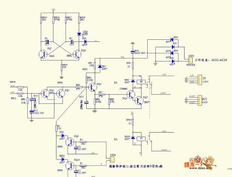
30A dual channel schematic diagram is shown as the figure.
(View)
View full Circuit Diagram | Comments | Reading(642)
Three Frequency Crystal Marker
Published:2012/12/10 0:40:00 Author:muriel | Keyword: Three , Frequency Crystal Marker

View full Circuit Diagram | Comments | Reading(648)
Phasing Exciter for 75 Meter SSB
Published:2012/12/10 0:40:00 Author:muriel | Keyword: Phasing Exciter, 75 Meter SSB

View full Circuit Diagram | Comments | Reading(1440)
Digital Responder timing design circuit
Published:2012/12/10 0:29:00 Author:Ecco | Keyword: Digital Responder , timing

According to the difficulty degree of the grab answer, the host will set the time to answer the question, and the counter is set by preset by preset time circuit, and the counter clock pulse is provided by the second pulse circuit. The preset time circuit is designed by decimal synchronization addition and subtraction counter 74LS192 circuit, and the specific circuit is shown as the figure.
(View)
View full Circuit Diagram | Comments | Reading(1817)
Optical isolation device transmission linearity improving circuit diagram
Published:2012/12/10 0:21:00 Author:Ecco | Keyword: Optical isolation , transmission linearity, improving

It uses negative feedback techniquesto greatly improve the transmission photocoupler linearity.
In figure (a), D1 is in the feedback path, the current flowing D1 has the linear relationship with Vi. The disadvantage of this circuit is not taken into account the non-linear relationship between the current transfer ratio of optocoupler devices and operating current. Therefore, the deviced must be carefully selected.
(View)
View full Circuit Diagram | Comments | Reading(1023)
Microcomputer data acquisition system circuit diagram
Published:2012/12/10 0:15:00 Author:Ecco | Keyword: Microcomputer, data acquisition system

Microcomputer data acquisition system composed of AD570, AD1408 and microprocessor CPU8155 circuit is shown as the figure. The measuring circuit has eight channels, each channel has sequential measurements, the scanning of each channel does not exceed 50μs, the system logic levels use TTL, binary code, data transmission way.
(View)
View full Circuit Diagram | Comments | Reading(1378)
Tms320f2812 dsp controller - based electric circuit diagram
Published:2012/12/7 0:58:00 Author:Ecco | Keyword: dsp controller, electric

Tms320f2812 dsp controller - based electric circuit diagram is shown in figure.
(View)
View full Circuit Diagram | Comments | Reading(860)
Optocoupler output mode circuit diagram of switching power supply
Published:2012/12/7 0:56:00 Author:Ecco | Keyword: Optocoupler , output mode , switching power supply

The PWRGD output port of power supply can display the input state of external power supply, and it is shown in Figure 1.
(View)
View full Circuit Diagram | Comments | Reading(1113)
Data used to produce transconductance for the FET used in our sample amplifier.
Published:2012/12/6 20:07:00 Author:muriel | Keyword: Data, produce transconductance, FET, sample amplifier.


View full Circuit Diagram | Comments | Reading(625)
Basic behavior of an N-Channel depletion mode JFET
Published:2012/12/6 20:06:00 Author:muriel | Keyword: N-Channel , depletion mode, JFET


View full Circuit Diagram | Comments | Reading(779)
JFET BIASING TUTORIAL
Published:2012/12/6 19:56:00 Author:muriel | Keyword: JFET


View full Circuit Diagram | Comments | Reading(718)
Voltage Variable Capacitance (VVC) Diodes
Published:2012/12/6 19:54:00 Author:muriel | Keyword: Voltage Variable Capacitance (VVC), Diodes

View full Circuit Diagram | Comments | Reading(954)
Silicon and Zener Diodes
Published:2012/12/6 19:54:00 Author:muriel | Keyword: Silicon and Zener Diodes

Silicon diodes are widely available and inhabit almost every junk box. I have tried using many types of diodes as voltage variable capacitors, but some types, such as rectifier diodes have a better range of variable capacitance than others. As stated before, reversed-biased diodes will decrease in capacitance as the voltage applied to them is increased. Do not expect the Q and thus the stability of a tuned circuit using silicon diodes to be that of better VVC diodes in a similar circuit. One particularly practical example of an application for using silicon diodes is for BFOs. In a BFO, there is typically a crystal and the desired frequency change is relatively small making silicon diodes attractive as the tuning device.
Earlier, I referred to W6WTUs HAM Radio Magazine article. From my own experiments, I confirmed Hugh's readings and found that rectifier diodes, are probably the most practical and easy silicon diodes to use as voltage variable capacitors. As far as rectifiers diodes go, the 1N4001 is probably the most commonly used in this application and a web search of HAM Radio electronic sites found its use in three different oscillator projects. From my experiment, the 1N4001 may exhibit a capacitance swing from 35 pF to 4 pF with a corresponding minimum and maximum reverse DC voltage of 0.5 and 12.0 volts. If you increase the voltage above 12.0, a lower capacitance may be realized but its significance is limited as it is getting into the non-linear area of the voltage versus capacitance curve and above normal QRP operating voltages. In addition, the linearity of the change in capacitance versus reverse voltage change is quite poor under ~5 volts for the 1N4001. I plotted the response curve for the 1N4001 and the results indicated that the best control voltage range to use for VFO tuning linearity is 5.0 to 12.0 volts. (View)
View full Circuit Diagram | Comments | Reading(759)
Bipolar Junction Transistors 2
Published:2012/12/6 19:52:00 Author:muriel | Keyword: Bipolar Junction Transistors

Experiments were conducted on this circuit and the minimum and maximum frequency and corresponding measured DC voltage on the BJT emitters for each was recorded. In Figure 4 as shown, the lower frequency/DC voltage was 7.054 MHz and 1.08 volts and the upper frequency/voltage was 7.062 MHz and 6.52 volts.
In the red insets are a schematic showing a four BJT version of this circuit and a plot of the reverse voltage versus frequency of the Figure 4 VFO without the series 22K and grounding 10K resistor ( This accounts for the frequency differences between the plot and the final VFO ). As shown, the best tuning linearity is above 3 volts, however, that would limit the tuning range too much and I chose components to give a voltage swing from 1.08 volts to 6.52 volts. With this particular arrangement the maximum voltage was limited with the 9.1 volt zener and series 22K resistor as the zener (breakdown) voltage on the EB junction of a 2N3904 is close to 8 or 9 V and you never want to lose the reverse bias and go into breakdown. (View)
View full Circuit Diagram | Comments | Reading(665)
Bipolar Junction Transistors
Published:2012/12/6 19:52:00 Author:muriel | Keyword: Bipolar Junction Transistors

VVC diodes may not be in your junk box. For popcorn VFOs, if you really want to save money on a parts order, bipolar transistors such as the 2N3904 may be used as voltage variable capacitors for a popcorn receiver project. Only two leads on the transistor are ever used and the redundant lead maybe cut off. Voltage variable capacitors using one, two or four BJTs may be used depending on the tuning range and popcorn factor you desire. It is obvious that the Q of a BJT tuning diode will not be as high as those seen in better VVC diodes, but they are practical alternatives for very low-cost, simple receiver projects. I would probably not use a BJT-tuned VFO to tune a transmitter project as the potential for drift is high, however reasonable stability is possible with careful design and a bit of luck.
Consider Figure 3. For brevity sake, the VFO buffer stages will not be shown any more but were used in all of the Figures to follow. A single 2N3904 is used as the variable tuning capacitor in this experiment. Note that there are two voltage regulators used on this schematic. If you were really going frugal, only one could also be used. The voltage regulator on the nJFET of the Hartley oscillator is used to lower its operating voltage to minimize the effects of internal heating on this device which can cause drift. Also keeping the RF amplitude down in a PN-junction turned circuit is probably a good idea as large AC voltage swings may cause the PN junction of our tuning device to conduct and reduce Q and waveform purity. You can always build up the oscillator output voltage with buffer/amplifiers.
The second zener diode voltage regulator is used on the voltage control circuit of the tuning circuit. Unregulated voltage for the tuning device whether it is a transistor or diode is not recommended as fluctuations in DC supply voltage will change the frequency of the VFO. Additionally, your DC tuning voltage must be free of any ripple, hum or noise riding along the DC voltage. AC noise if present, can sweep the oscillator frequency at a rate consistent with the ripple frequency. Clean DC power may be achieved by decoupling your VFO power supply from RF with RF chokes, resistors and capacitors. It is also good practice to ensure that correct polarity to your VFO circuit is present at all times.
You can not eliminate the series 100 pF NP0 ceramic capacitor connecting the 2N3904 to the tank circuit or the VFO will not oscillate. You can however, experiment with this capacitor value.
Figure 3 contains the minimum tuning voltage and frequency measured in the test VFO. The capacitance of the 2N3904 will be at its maximum level at the minimum control voltage. The frequency and voltage with the pot turned all the way to the left is 7.036 MHz and 5.82 volts respectively. The minimum control voltage is set by the 47K resistor connecting the 50K pot to ground. Raising this value will raise the minimum control voltage and lowering or eliminating this resistor will lower the control voltage. When the 47K resistor was removed, the measured voltage was 3.42 volts which gave a minimum frequency of 6.977 MHz. From Figure 2 we learned that the minimum voltage should be 7 volts for maximum linearity in the VFO tuning response. I decided to accept 5.82 volts as a trade off to illustrate that in many cases you may compromise the minimum tuning voltage to suit the standard value resistors you have on hand or to attain a bigger tuning range for your VFO. In many design scenarios, compromises may be made to suit your needs and parts collections! The maximum control voltage is largely set by the 11.7 volt zener diode. If you wished to lower this value series resistors or a voltage divider could be added as well. The 11.7 volt zener was chosen as I may want to use this VFO with a 12 volt battery and this zener diode would facilitate such operation. The maximum control voltage and frequency with the pot turned all the way to the right is 7.053 MHz and 11.88 volts. The 2N3904's capacitance would be at its minimum value for this circuit at 11.88 volts. The Figure 3 VFO tuning range is 17 KHz, with the control voltage going from 5.82 to 11.88 volts.
The stability of this VFO is fair. I have a commercial kit receiver that has worse drift, but again I would hesitate to use this VFO design for a transmitter.
One of the drawbacks of using just a single tuning diode or BJT is that if the device is forward biased by the RF signal during part of the AC cycle, it's reverse leakage will increase momentarily and it's Q will be reduced. Also, harmonic energy is produced as the tuning diode or BJT is alternately biased positive and negative which results in reduced VFO output waveform linearity. The solution is to connect two tuning diodes or BJTs back to back with the reverse DC voltage applied to both devices simultaneously. The two tuning diodes will be driven alternately into high and low capacitance and the net capacitance will remain constant and not be affected by the AC signal amplitude. The circuit in Figure 3 could be improved by adding another 2N3904 back-to-back with the existing one, but the tuning range will be reduced. This occurs because you have now connected two capacitors in series and the total capacitance has been reduced and may be analyzed by the classic capacitors in series equation we all learned in radio school. (View)
View full Circuit Diagram | Comments | Reading(1415)
NPN DC-BIAS
Published:2012/12/6 1:26:00 Author:muriel | Keyword: NPN DC-BIAS
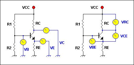
This application calculates the various voltages and currents of a simple voltage divider bias NPN bipolar transistor amp. The following is calculated: IB, IC, IE, VE, VB, VC, VCE and detection of Saturation or Cutoff. The user can alter the VCC, VBE, transistor beta and any of four resistor values R1, R2, RC and RE by picking the transistor value from a standard-value resistor table or manually entering the value. The schematic illustrates some of the voltage measuring points on the transistor schematic. This app is in final BETA. (View)
View full Circuit Diagram | Comments | Reading(841)
USB digital I/O extender
Published:2012/12/6 1:13:00 Author:muriel | Keyword: USB , digital I/O extender

View full Circuit Diagram | Comments | Reading(1312)
Discriminant analysis methods for high - voltage capacitor
Published:2012/12/5 21:33:00 Author:Ecco | Keyword: Discriminant analysis methods, high - voltage capacitor

As shown in Figure a), touching the capacitor lead end, if there is a strong spark generated, this capacitor is good; if there is no spark, this capacitor has been damaged or a minimum capacity. Figure b) is used to test the capacity of the capacitor. Read out the reading on the two tables of PA, PB, the capacitor capacitance can be obtained according to the following formula. C = 3180 * Ic / Uc, C (μF ) , Ic (A ) , UC ( V ).
(View)
View full Circuit Diagram | Comments | Reading(589)
Simple phase sequence indicator
Published:2012/12/5 21:36:00 Author:Ecco | Keyword: Simple , phase sequence, indicator


As shown in figure, as long as the X, Y, Z three lines are connected to three - phase circuit, the phase sequence of three - phase alternating current can be easily seen by the quenching of the neon tube light. If neon tube is lit , X , Y , and Z are respectively connected to A, C, B power supply phases. Conversely, if the neon tube is not lit, then the X , Y, and Z are connected to power supply A , B, and C phases. 1/8W carbon film resistors can be used, and the capacitor requires that the pressure to be greater than 400V. Neon can use neon fluorescent starter.
(View)
View full Circuit Diagram | Comments | Reading(4027)
External audio spectrum monitor circuit diagram
Published:2012/12/3 21:25:00 Author:Ecco | Keyword: External, audio spectrum monitor

Generally top-grade audio equipment has audio spectrum display device which can not only help know instantaneously the playback signal spectrum, but also has the elegant and beautiful visual effects. This external audio spectrum display described here doesn't need any electrical stereo equipment, if irt is simply placed in the speaker front the voice box, it can visually dynamically show the frequency spectrum of the audio signal with nice and good looking. All the displays use integrated operational amplifiers and ASIC in design.
(View)
View full Circuit Diagram | Comments | Reading(1127)
| Pages:64/471 At 206162636465666768697071727374757677787980Under 20 |
Circuit Categories
power supply circuit
Amplifier Circuit
Basic Circuit
LED and Light Circuit
Sensor Circuit
Signal Processing
Electrical Equipment Circuit
Control Circuit
Remote Control Circuit
A/D-D/A Converter Circuit
Audio Circuit
Measuring and Test Circuit
Communication Circuit
Computer-Related Circuit
555 Circuit
Automotive Circuit
Repairing Circuit