
Basic Circuit
Index 63
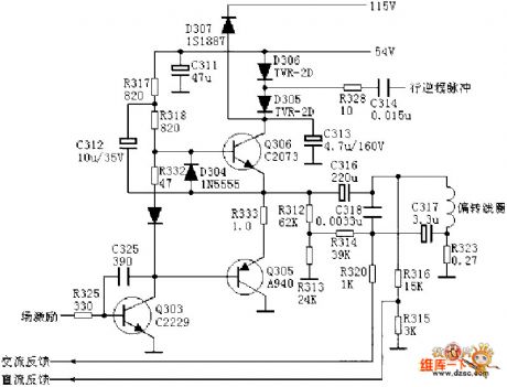
Pseudo-Random Number Generator
Published:2012/12/17 20:24:00 Author:muriel | Keyword: Pseudo-Random, Number Generator

View full Circuit Diagram | Comments | Reading(1416)
Isolation and directly driving CW1840 driver MOS tube circuit diagram
Published:2012/12/17 2:36:00 Author:Ecco | Keyword: Isolation , directly driving , driver, MOS tube
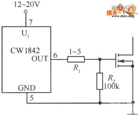
Isolation and directly driving CW1840 driver MOS tube circuit diagram is shown as the figure.
(View)
View full Circuit Diagram | Comments | Reading(666)
Field output circuit : TDA3654 circuit diagram
Published:2012/12/15 2:20:00 Author:Ecco | Keyword: Field output
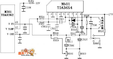
TDA3654 is a field output circuit which can drive deflection angle system, and its current is up to 1.5A ( PP ) with overheating, overload protection.
(View)
View full Circuit Diagram | Comments | Reading(5702)
Field output circuit: TA8403 circuit diagram
Published:2012/12/15 2:23:00 Author:Ecco | Keyword: Field output

Pin 1: 0V - groundPin 2: 12.4V-- field outputPin 3: 25V - farm output stage power supplyPin 4: 1.0V-- field excitation signal inputPin 5: 0.6V-- phase compensationPin 6: 24V - powerPin 7: 1.5V - - pump power output
(View)
View full Circuit Diagram | Comments | Reading(2490)
Field output circuit: TA8427 circuit diagram
Published:2012/12/15 2:25:00 Author:Ecco | Keyword: Field output
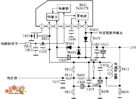
Pin 1: 0V - groundPin 2: 14V-- field outputPin 3: 27V - farm output stage power supplyPin 4: 1.0V-- field excitation signal inputPin 5: 0.6V-- phase compensationPin 6: 27V - powerPin 7: 1.9V - - pump power output
(View)
View full Circuit Diagram | Comments | Reading(1032)
Field output circuit: OTL discrete circuit diagram
Published:2012/12/15 2:38:00 Author:Ecco | Keyword: Field output, OTL discrete
The output circuit composed of OTL discrete components is widely used in various brands of machines (generally under 25 or 25-inch machine), the circuits are different, but circuit programs are exactly the same.
(View)
View full Circuit Diagram | Comments | Reading(1026)
Field output circuit : LA7838 circuit diagram
Published:2012/12/15 2:17:00 Author:Ecco | Keyword: Field output
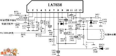
Pin 1: 9.2V-VCC1 powerPin 2: 4.8V-vertical trigger inputPin 3: 4.8V-monostable multivibrator oscillation time constant setting endPin 4: 4.8V-field amplitude control terminalPin 5: 0.5V-50/60HZ conversion field amplitude stability control terminal (50HZ: L 60HZ: H)Pin 6: 4.8V-sawtooth voltage form endPin 7: 4.6V-- farm output AC and DC feedback inputpin 8: 24.5V-VCC2 powerPin 9: 1.9V-pump power outputPin 10: 1.5V-anti- self -excited negative feedback inputPin 11: 0V - groundPin 12: 15V - field scanning outputPin 13: 24V - farm output power
(View)
View full Circuit Diagram | Comments | Reading(6471)
half-shot circuit
Published:2012/12/14 20:50:00 Author:muriel | Keyword: half-shot circuit
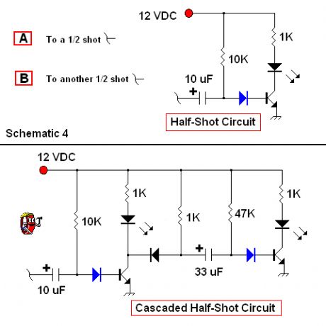
View full Circuit Diagram | Comments | Reading(1108)
Digital alarm clock circuit diagram
Published:2012/12/14 0:29:00 Author:Ecco | Keyword: Digital alarm clock

U1 is the 3817 integrated circuit. It has the ability to drive the display directly, and it can display 12h or 24h, schedule alarm sounds, timely and automatically turn on the radio. Display is FND500 light-emitting diode, the input frequency is 50H or 60Hz. U2 is the 7800 series regulator, its rated power can meet the requirements of the radio. Users can select radio playing time length ( the maximum is 59 min), then Q3 will output a low level to automatically turn off the radio.
(View)
View full Circuit Diagram | Comments | Reading(5591)
UC3907 one-way buffer replacing diode circuit diagram
Published:2012/12/14 0:23:00 Author:Ecco | Keyword: one-way buffer, replacing diode
This can reduce the impact on the current precision of of the main module from diode forward voltage drop. The circulation between the main module and other modules is reduced to 2.5% or less.
(View)
View full Circuit Diagram | Comments | Reading(899)
popcorn crystal filter
Published:2012/12/13 21:33:00 Author:muriel | Keyword: popcorn crystal filter

View full Circuit Diagram | Comments | Reading(1117)
10MHz crystalk bandpass RF filter
Published:2012/12/13 21:32:00 Author:muriel | Keyword: 10MHz, crystalk bandpass, RF filter

View full Circuit Diagram | Comments | Reading(1493)
10 MHz, double tuned RF band pass filter
Published:2012/12/13 21:30:00 Author:muriel | Keyword: 10 MHz, double tuned, RF band, pass filter

View full Circuit Diagram | Comments | Reading(3838)
Experiments with JFET Biasing
Published:2012/12/13 21:25:00 Author:muriel | Keyword: Experiments, JFET Biasing

View full Circuit Diagram | Comments | Reading(655)
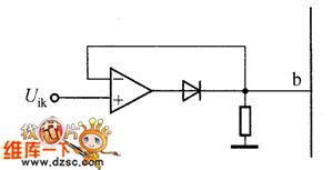
Voltage positive pulse peak holding circuit diagram
Published:2012/12/13 0:51:00 Author:Ecco | Keyword: Voltage, positive pulse, peak holding

Voltage positive pulse peak holding circuit diagram is shown as below:
(View)
View full Circuit Diagram | Comments | Reading(1447)
The internal structure schematic diagram of UC3907 IC chip
Published:2012/12/13 1:00:00 Author:Ecco | Keyword: internal structure , IC chip
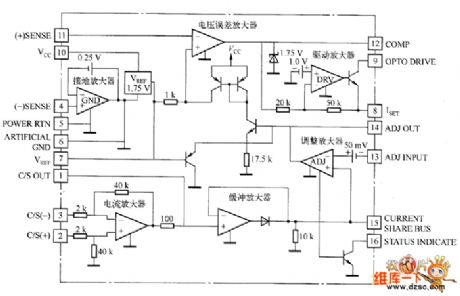
Operating supply voltage range V (10 feet) is 4.5 ~ 35 V; chip has a reference voltage source VREF, and its value relative to ARTIFICIAL GND (6 feet ) is 1.15 V which can output from VREF (7 feet ); ARTIFICIAL GND is the low resistance ground ( ground reference ) of chip, and its level is higher 0.25V than (-) SENSE (4 feet), and the voltage bias provides loop circuit for the the grounded amplifier current, while the voltage sampling negative terminal ( - ) Sense ( i.e. grounded amplifier inverting input terminal ) has a high input impedance.
(View)
View full Circuit Diagram | Comments | Reading(1556)
The FM optical receiver circuit diagram
Published:2012/12/13 0:49:00 Author:Ecco | Keyword: FM , optical receiver
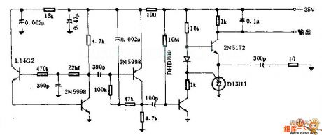
This circuit is applied to the pulse rate modulation system. In this system, the transmitter changes the pulse rate of modulated light speed in optical fiber, so that the vertical variation is around the frequency of 50kHz center. L14G2 phototransistor converts modulated light to RF signal to restore the original audio signal.
(View)
View full Circuit Diagram | Comments | Reading(1184)
The connection schematic block circuit diagram of UC3907 and external circuit
Published:2012/12/12 3:27:00 Author:Ecco | Keyword: connection , external circuit
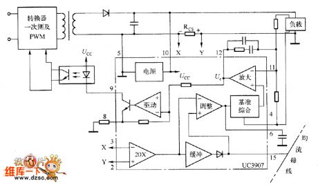
Current signal is sampling by an external shunt, RCS is generally connected with return branch in series, and it is sent to current amplifier by pin 2 and pin 3, the output voltage of the power module input uses by 11 feet and 4 feet differential signal, and it is superimposed with circulation.
(View)
View full Circuit Diagram | Comments | Reading(749)
82C250 functional block circuit diagram
Published:2012/12/12 2:58:00 Author:Ecco | Keyword: functional block
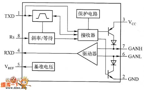
Figure 1 shows a functional block diagram between CAN controller and interface circuit 82C250 of physical bus. 82C250 is able to provide differential receive and transmit functions for bus to achieve electrical isolation between each node on the bus, and the maximum transmission rate is up to 1 Mb / s.
(View)
View full Circuit Diagram | Comments | Reading(1053)
Solid State Tesla Coil Circuit
Published:2012/12/12 0:20:00 Author:muriel | Keyword: Solid State , Tesla Coil Circuit

View full Circuit Diagram | Comments | Reading(1295)
| Pages:63/471 At 206162636465666768697071727374757677787980Under 20 |
Circuit Categories
power supply circuit
Amplifier Circuit
Basic Circuit
LED and Light Circuit
Sensor Circuit
Signal Processing
Electrical Equipment Circuit
Control Circuit
Remote Control Circuit
A/D-D/A Converter Circuit
Audio Circuit
Measuring and Test Circuit
Communication Circuit
Computer-Related Circuit
555 Circuit
Automotive Circuit
Repairing Circuit