
Basic Circuit
Index 72
Grating circuit with Schmitt Trigger
Published:2012/9/27 21:25:00 Author:Ecco | Keyword: Grating , Schmitt Trigger
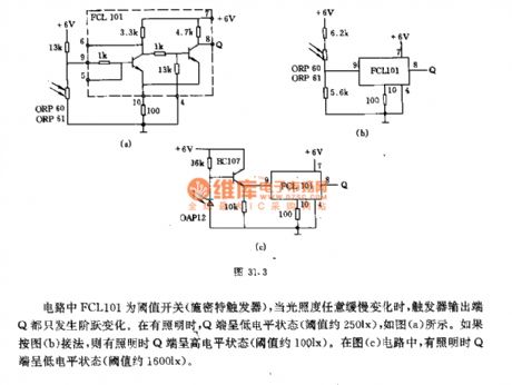
The FCL101 in circuit is a threshold switch (Schmitt trigger), when the illumination changes arbitrarily and slowly, the flip - flop's output terminal Q occurs step change. When there is lighting, the Q end is in low level (threshold is about 250lx ), and it is shown in Figure a. If it is connected like Figure b, the Q terminal is in high level when there is lighting ( threshold value approximately 100lx. In the circuit shown in FIG c, Q-side is in lowlevel (threshold value is approximately 1600lx ).
(View)
View full Circuit Diagram | Comments | Reading(836)
The reducing and cut-off frequency circuit with capacitor( wideband strain signal conditioner 1B31)
Published:2012/9/26 22:29:00 Author:Ecco | Keyword: reducing , cut-off frequency , capacitor, wideband , strain signal , conditioner


The external capacitors CSEL1 and CSEL2 can set cutoff frequency of low pass filter below 1kHz to meet the needs of the application of narrowband, and the circuit is shown in Figure. The capacitance is calculated as following:
(View)
View full Circuit Diagram | Comments | Reading(906)
The excitation voltage enhancing circuit ( broadband strain signal conditioner 1B31 )
Published:2012/9/26 21:22:00 Author:Ecco | Keyword: excitation voltage , enhancing circuit, broadband strain , signal conditioner


When broadband strain signal conditioner 1B31's pin 19 connects to pin 20, the excitation voltage output by programmable bridge excitation source UEXC = +10 V. In order to upgrade UEXC to +10 ~ +15 V, it must be connected to a resistor REXT between the XC ADJ end and SENSE- end, the circuit is shown in the figure. REXT value is determined by the following formula ( resistance units kΩ):
(View)
View full Circuit Diagram | Comments | Reading(818)
The typical application circuit of digital output - angle sensor signal conditioner UZZ9001
Published:2012/9/26 21:27:00 Author:Ecco | Keyword: typical application , digital, output - angle sensor , signal conditioner

The UZZ9001 typical application circuit is shown in figure. C is the decoupling capacitor. SPI input / output interfaces can be directly matched with the microcontroller (μC), it uses single-chip to set UZZ9001. UZZ9001 measuring angle error is about ± 0.35°.
(View)
View full Circuit Diagram | Comments | Reading(1058)
The bus structure layout of low-power programmable sensor signal processor TSS400-S2
Published:2012/9/26 21:52:00 Author:Ecco | Keyword: bus structure layout , low-power programmable sensor, signal processor

TSS400-S2 bus system allows one-way communication in a two-wire bus. The bus can use twisted pair. Under the request of host machine, the data can be transmitted from slave to host machine. When the bus is effective, the slave machine can start asynchronous data transmission. TSS400-S2's bus structure layout is shown in Fig. This circuit uses a Bus Interface circuit TSS721. It uses ENBUS instruction to complete the slave module remote reading.
(View)
View full Circuit Diagram | Comments | Reading(851)
The interface circuit between 5-channel low-power programmable sensor signal processor AD7714 and DSP
Published:2012/9/26 22:25:00 Author:Ecco | Keyword: interface , 5-channel , low-power programmable sensor , signal processor, DSP

ADSP-2103 or ADSP-2105 is the digital signal processor produced by ADI. The interface circuit between AD7714 and ADSP-2103/2105 is shown as the chart. If ADSP-2103/2105 RFS non-end and TES non- end are configured as low level, the output is effective, then SCLK end is configured as serial clock output. The AD7714 's POL termination is connected to low level. In order to ensure that the AD7714 can work normally, ADSP-2103/2105 serial clock frequency should be limited to less than 3MHz.
(View)
View full Circuit Diagram | Comments | Reading(695)
The proximity switch circuit with integrated magnetic field sensor HMC1001
Published:2012/9/25 21:25:00 Author:Ecco | Keyword: proximity switch , integrated , magnetic field, sensor

As shown in figure, the proximity switch circuit is composed of HMC1001, operational amplifier (AMP04) and light emitting diode (LED). The operational amplifier is used as a comparator. When you move magnet with length being 6mm~12mm to HMC1001 in a predetermined position, the output voltage of MR bridge will reach 30mV, then the comparator flips, and output becomes a low level to light LED. If the magnet is removed, the comparator outputs high level to turn off LED. Obviously, the circuit is equivalent to the proximity switch of indicator light, and it can be used to detect displacement, rotate speed and other non-electricity. Adjusting R1 can set the threshold voltage of the switch.
(View)
View full Circuit Diagram | Comments | Reading(2177)
The interface circuit of pressure transmitter ( wideband strain signal conditioner 1B31)
Published:2012/9/25 21:35:00 Author:Ecco | Keyword: interface , pressure transmitter , wideband, strain signal , conditioner

The interface circuit between typical pressure transmitter ( such as Dynisco's 800 series of pressure transmitter ) and 1B31 is shown as the figure. 1B31 outputs +10 V excitation voltage, the pressure transmitter outputs 30mV voltage in full scale. The gain of 1B31 is set 333.3 times to convert the 0 to 10,000 pounds / inch 2 pressure into 0 ~ 10V output. In order to eliminate ground loop, the signal return side and shielded cable must be grounded in the same place. S is the calibration switch, R is the branch calibration resistor to calibrate 80 % of full-scale output point.
(View)
View full Circuit Diagram | Comments | Reading(1401)
The bridge excitation circuit of digital pressure signal conditioner MAX1458
Published:2012/9/25 21:46:00 Author:Ecco | Keyword: bridge excitation , digital pressure, signal conditioner

It uses DAC3 output to change the size of the sensor excitation current IBR and achieve fine full-scale calibration. IISRC is reference current which is set by RISRC and the voltage of pin 9. V1 and V2 form a mirror current source, and the current gain is 14 times which enables the excitation current IBR = 14IISRC. The IBR programming range is 0.1 ~ 2mA. The on-off state of analog switches S1, S2 is governed by the configuration register. Obviously, when the full-scale output voltage changes, DAC3 can compensate bridge output voltage by changing BR, thereby correcting the errors of the full scale. DAC4 is used to correct the error of full scale temperature coefficient.
(View)
View full Circuit Diagram | Comments | Reading(735)
Application circuit diagram of pulse width modulator LZ210
Published:2012/9/25 21:51:00 Author:Ecco | Keyword: Application , pulse width modulator


LZ210 is a dedicated long cycle pulse width modulator circuit,and it can convertthe voltage amplitude into a corresponding pulse width variations, and it is used withmatching with zero crossing trigger.The electrical parameters are shownas following:Supply Voltage: DC +15 V.Supply Current : ≤ l2mA.Ramp rate : ≥ 8V ( test conditions : Vcc = 15V)Control voltage:a. 0 ~ +8 V b. -4 ~ +4 VC. -8 ~ 0V d. -8 ~ +8 VOscillation cycle oscillation cycle : When Vcc = 15V, RT = 100kΩ ( see Figure 2-26 ).T = 0.06 ~ 0.12 ms (C t = 200p)T = 9 ~ 76 ms (C t = 0.1μ)T = 1 ~ 800 ms (C t = 1μ)T = 900 ~ 6 400ms (C t = 10μ)T = 24 000 ~ 120 000ms (C t = 220μ)The LZ210 uses 8-pin dual in-line package, and it isshown in the figure.
(View)
View full Circuit Diagram | Comments | Reading(960)
Variable Zener Diode
Published:2012/9/25 21:38:00 Author:muriel | Keyword: Variable, Zener Diode

This variable Zener diode circuit acts like a Zener diode with a breakdown voltage adjustable in a vast domain. The current through the voltage divider R1 and R2 must be higher current through the voltage divider should be higher compared with that of the transistors base. It depends only by R1 and has been set to 8 mA. The breakdown voltage of this simulated Zener diode is adjustable between 5V and 45V. The circuit begins to stabilize at a current of 15 mA. The maximum current for a Zener is 4.7V/250mW is around 50 mA.
If you need to stabilize voltages above 15V, the transistor must be mounted on a heatsink. This measure must be taken if the current consumption of the circuit reaches 40-50 mA.
Variable Zener Circuit Schematic
(View)
View full Circuit Diagram | Comments | Reading(2312)
The Schmitt trigger circuit with hysteresis comparator
Published:2012/9/24 22:17:00 Author:Ecco | Keyword: Schmitt trigger , hysteresis comparator

Figure a shows the basic circuit.
Figure b shows hysteresis and insensitive zone.
Figure c shows the output wave withouthysteresis.
Figure d shows the output wave withhysteresis.
(View)
View full Circuit Diagram | Comments | Reading(1441)
Schmitt trigger circuit with inverting and non-inverting output
Published:2012/9/24 22:08:00 Author:Ecco | Keyword: Schmitt trigger , inverting , non-inverting output


Schmitt trigger is a bistable circuit, when the input exceeds a certain value UE1, it flips and restores the original state until UE2, so it can shape any input waveform to the square wave with a certain amplitude. It uses integrated circuit TCA965 to achieve this function. Compared to using a single transistor or Schmitt trigger with operational amplifier, the advantage is that the threshold and hysteresis can be adjusted independently by potentiometers RP1 and RP2.
(View)
View full Circuit Diagram | Comments | Reading(1555)
The logarithm table circuits using operational amplifier
Published:2012/9/24 20:57:00 Author:Ecco | Keyword: logarithm table, operational amplifier

The circuit shown in Fig a can select NPN or PNP transistor in accordance with the polarity of the input signal, and its zero voltage can be adjusted by the potentiometer RP.The circuit shown in Figure b can be used as logarithm table, and its transistor can also select NPN or PNP according to polarity.
(View)
View full Circuit Diagram | Comments | Reading(771)
Resistor to raise the cutoff frequency ( broadband strain signal conditioner 1B31)
Published:2012/9/23 22:54:00 Author:Ecco | Keyword: Resistor , raise, e cutoff frequency , broadband , strain , signal conditioner
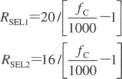

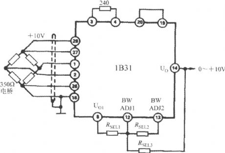
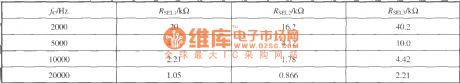
The cutoff frequency can be increased from 1kHz to 20kHz to meet the needs of broadband applications by three external resistors. The circuit is shown as the figure.
The unit of RSEL1 ~ RSEL3 istaken kΩ.The resistor valuealso can be directlyselected according to the following table.
(View)
View full Circuit Diagram | Comments | Reading(701)
Three - phase AC voltage regulator circuit diagram for KCZ6 component applications
Published:2012/9/23 22:41:00 Author:Ecco | Keyword: Three - phase , AC voltage , regulator, component applications

The pulse transformer can used Mn-Zn ferrite pot.It generally usesSEAR2: l pulse transformer with U30 core.
(View)
View full Circuit Diagram | Comments | Reading(4449)
The series circuit with many TcA965
Published:2012/9/23 22:51:00 Author:Ecco | Keyword: series circuit
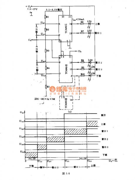
In many measuring instruments, they often require more than three of measuring ranges, and they are able to display and monitor. As shown in Figure, the series circuit composed of many window discriminators can be used. There are five ranges, i.e., three windows and an upper and a lower. They are adjusted through R1 ~ R5 dividers. Input signal UE is sent from pin 8. Figure b illustrates the pulse waveform. In actual applications, it can be used by five TCA965 connected in series.
(View)
View full Circuit Diagram | Comments | Reading(1280)
Typical Schmitt trigger circuit
Published:2012/9/23 22:29:00 Author:Ecco | Keyword: Typical , Schmitt trigger
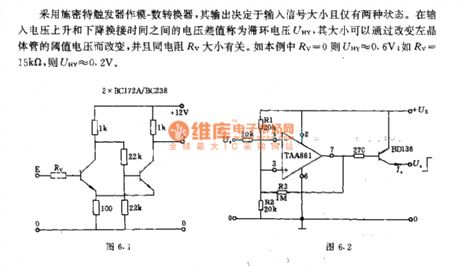
It uses Schmitt trigger for mode - digital converter, and the output depends on the input signal magnitude, and it only has two states. The voltage difference between the input voltage rising and falling the change-over time is known as the hysteresis loop voltage UNY, and its size can be changed by threshold voltage of the left transistor, and it is associated with the size of the resistance RV. Such as the present example, RV = 0 , UNY ≈ 0.6V; RV = 15kΩ, UHY ≈ 0.2V.
(View)
View full Circuit Diagram | Comments | Reading(949)
Photosensitive monostable trigger circuit
Published:2012/9/23 22:12:00 Author:Ecco | Keyword: Photosensitive , monostable trigger
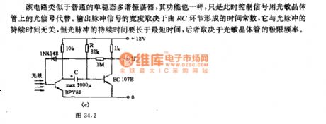
This circuit is similar to the ordinary monostable multivibrators, and their function is the same, but at this time, the control signal is replaced by optical signals on the phototransistor. The output pulse width of the signal depends on the time constant formed by the RC link, it has nothing to do with the duration of the light pulse which is longer than the shortest time, and the later depends on the limit frequency of the phototransistor.
(View)
View full Circuit Diagram | Comments | Reading(771)
Limiter and rectifier circuit using the operational amplifier
Published:2012/9/23 22:04:00 Author:Ecco | Keyword: Limiter , rectifier, operational amplifier
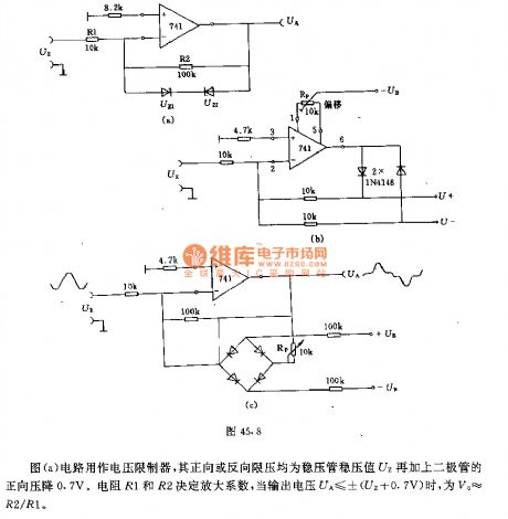
The circuit shown in Figure a is a voltage limiter, and its forward or reverse limit pressure is the zener regulator value UZ with adding 0.7V diode forward voltage drop. The resistors R1 and R2 determine the amplification coefficient, when the output voltage UA ≤ ± (UZ +0.7 V), V0 ≈ R2/R1.The circuit shown in Figure b can be used as a precision rectifier. It can output a positive or negative rectifier partial pressure according to the polarity requirements. It is often followed by the integrator in actual applications.Figure c shows the amplifier circuit with adjustable low input voltage and amplification factor. The size of dead zone can be adjusted by potentiometer.
(View)
View full Circuit Diagram | Comments | Reading(1107)
| Pages:72/471 At 206162636465666768697071727374757677787980Under 20 |
Circuit Categories
power supply circuit
Amplifier Circuit
Basic Circuit
LED and Light Circuit
Sensor Circuit
Signal Processing
Electrical Equipment Circuit
Control Circuit
Remote Control Circuit
A/D-D/A Converter Circuit
Audio Circuit
Measuring and Test Circuit
Communication Circuit
Computer-Related Circuit
555 Circuit
Automotive Circuit
Repairing Circuit