
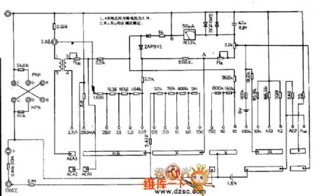
Index 390
MF77 multimeter circuit diagram
Published:2011/6/24 4:37:00 Author:Nicole | Keyword: multimeter

View full Circuit Diagram | Comments | Reading(1076)
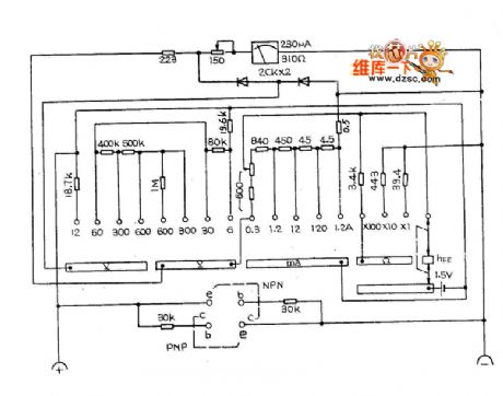
MF78 multimeter circuit diagram
Published:2011/6/24 4:41:00 Author:Nicole | Keyword: multimeter
View full Circuit Diagram | Comments | Reading(786)
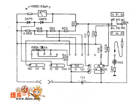
MF79 multimeter circuit diagram
Published:2011/6/24 4:41:00 Author:Nicole | Keyword: multimeter

View full Circuit Diagram | Comments | Reading(868)
MF81 multimeter circuit diagram
Published:2011/6/24 4:40:00 Author:Nicole | Keyword: multimeter
View full Circuit Diagram | Comments | Reading(624)
MF82 multimeter circuit diagram
Published:2011/6/24 4:40:00 Author:Nicole | Keyword: multimeter

View full Circuit Diagram | Comments | Reading(970)
MF75 multimeter circuit diagram
Published:2011/6/24 4:42:00 Author:Nicole | Keyword: multimeter
View full Circuit Diagram | Comments | Reading(696)
Electrical blaster 3
Published:2011/6/28 2:44:00 Author:Nicole | Keyword: Electrical blaster

The electrical blaster circuit is composed of delay switch circuit, insurance switch circuit, timing detonating circuit, charge indication circuit and detonating power supply circuit, it is shown in the figure 8-25.
The delay switch circuit is made of time base integrated circuit IC1, resistors R1, R2, potentiometer RP1, potentiometers C1-C3, diode VD1, thyristor VT1 and the contact S2-1 of detonating switch S2.
The insurance switch circuit consists of time base integrated circuit IC2, resistors R3, R4, potentiometer RP2, diode VD2, VD3, capacitors C4, C5, relay K and the contact S2-2 of S2.
(View)
View full Circuit Diagram | Comments | Reading(727)
Electrical blaster 2
Published:2011/6/28 2:33:00 Author:Nicole | Keyword: Electrical blaster
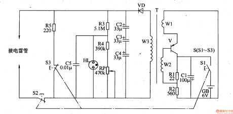
The electrical blaster circuit is composed of oscillator, boost circuit, charge indication circuit and discharge circuit, it is shown in the figure 8-24.
The oscillator is made of transistor V, capacitor C1, resistors R1, R2, battery GB, charge switch S1 and W1, W2 windings of boost transformer T.
The boost circuit consists of W3 winding of boost transformer T, rectifier diode VD and capacitors C2-C4.
The charge indication circuit is composed of resistors R3, R4, potentiometer RP, capacitor C5 and neon indication light HL.
The discharge circuit is made of discharge switch S2, drain switch S3 and resistor.
(View)
View full Circuit Diagram | Comments | Reading(922)
Single phase bridge type thyristor rectifier circuit
Published:2011/6/27 8:04:00 Author:Christina | Keyword: Single phase, bridge type, thyristor, rectifier circuit
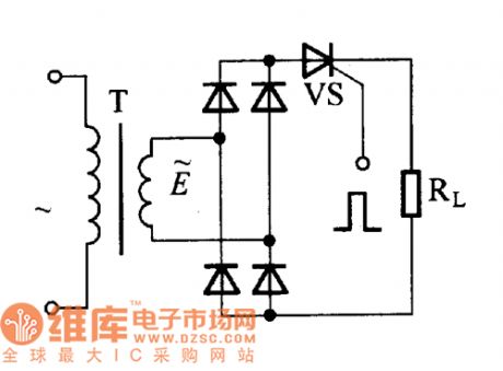

The single phase bridge type thyristor rectifier circuit is composed of the single phase bridge type rectifier circuit, the unidirectional thyristor and the load RL, as the figure shows. The single phase AC voltage is bridge-type rectified by this circuit and becomes the full-wave rectifier waveform. Because only when the trigger signal increases, the thyristor will conduct, and the thyristor is cut off when the AC voltage is crossing zero, so we can get the waveform which is as shown in figure (5). From the figure a and b, we can see that when the angle θ is small, the DC voltage average values at both ends of the load resistanceare small; when the angle θ increases, the DC voltage average values of the load resistanceare high.
(View)
View full Circuit Diagram | Comments | Reading(3789)
Three-phase bridge type thyristor rectifier circuit
Published:2011/6/27 7:37:00 Author:Christina | Keyword: Three-phase, bridge type, thyristor, rectifier circuit
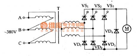
The three-phase bridge type thyristor rectifier circuit is as shown in the figure. The difference between this circuit and the three-phase bridge type rectifier circuit is: this circuit uses the unidirectional thyristor to replace the three rectifier diodes of the half bridge arm. You can change the thyristor conduction time of every cycle by changing the conduction angle θ of the three thyristors, and you can get the adjustable DC voltage average value. The three-phase bridge type thyristor rectifier circuit can be used in the speed regulation device of the high power DC motor.
Three-phase bridge type thyristor rectifier circuit (View)
View full Circuit Diagram | Comments | Reading(2262)
Partial voltage type negative feedback bias circuit
Published:2011/6/27 21:36:00 Author:Christina | Keyword: Partial voltage, negative feedback, bias circuit
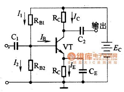
This circuit is designed as one kind of bias circuit, the typical circuit is as shown in the figure. In this circuit, the transistor emitter is connected with the RE, and the base electrode is connected with the RB1 and RB2.
Figure Partial voltage type negative feedback bias circuit
The partial voltage type negative feedback bias circuit has two kinds of stable effects:
1. Through the partial voltage of the base resistance RB1 and RB2, this relation is founding:
I2=I1-IB≈I1
UB=Ec-I1RB1
UB=I2xRB2
2.If you add the RE in this circuit, this circuit will have the function of current negative feedback temperature compensation.
Because of the two stable functions, this partial voltage type negative feedback bias circuit has good stable function. (View)
View full Circuit Diagram | Comments | Reading(598)
Current negative feedback bias circuit
Published:2011/6/28 1:29:00 Author:Christina | Keyword: Current, negative feedback, bias circuit
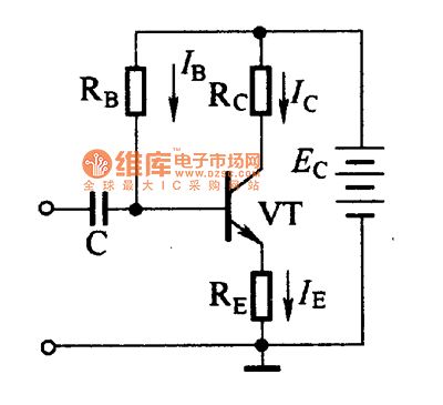
The current negative feedback bias circuit is as shown in the figure. The difference between this circuit and the fixed bias circuit is the semiconductor transistor emitter is connected with a resistance RE. The parameters of this circuit are: Ec=IERE+UBE+IBRB.
As the EC power is constant, if the IERE increases, the UBE will decreases, so the IB decreases too. The process of the circuit stable quiescent operating point is:
↑-->Ic↑-->IE↑-->IERE↑-->UBE↓-->IB↓-->IC↓
Figure: Current negative feedback bias circuit
(View)
View full Circuit Diagram | Comments | Reading(740)
AN5026K infrared remote control signal receiving integrated circuit
Published:2011/6/30 6:39:00 Author:Christina | Keyword: infrared, remote control signal, receiving integrated circuit
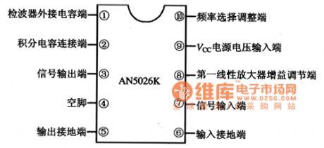
The AN5026K infrared remote control signal receiving integrated circuit is produced by the Panasonic company that can be used in all kinds of electronic products' remote control systems such as the remote control fans, air conditioners, acoustics, TVs, DVD players.etc.
1.Features
The AN5026K is composed of the preamplifier circuit, the bandpass filter circuit, the automatic level control circuit, the wave detection circuit and the buffer amplification circuit.
2.Pin functions and data
The AN5026K uses the 10-pin dual-row DIP package, the pin functions and data are as shown in figure 1, the operating parameters are as shown in table 1.
Figure 1 The pin functions and data of the AN5026K
Table 1 The operating parameters of the AN5026K
(View)
View full Circuit Diagram | Comments | Reading(463)
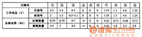
AN5179NK intermediate frequency signal processing integrated circuit
Published:2011/6/30 4:43:00 Author:Christina | Keyword: intermediate frequency, signal processing, integrated circuit
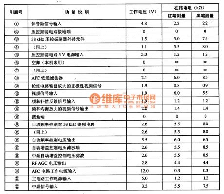
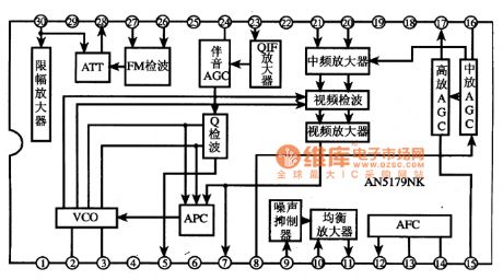
The AN5179NK intermediate frequency signal processing integrated circuit is produced by the Panasonic company, and it can be used in the Panasonic TV sets.
1.Features
The AN5179NK uses the audio-visual standard separation mode and it can be used in the multi-channel audio circuit. The AN5179NK integrates the alto AGC, the high pitch AGC, the automatic frequency control circuit and the audio circuit.
2.Pin functions and data
The AN5179NK uses the 30-pin dual-row DIP package, the pin functions and data are as shown in table 1.
Table 1. The pin functions and data of the AN5179NK
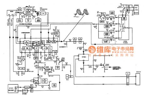
3.The internal circuit block diagram and the typical application circuit
The internal circuit block diagram and the typical application circuit are as shown in figure 1 and 2.
Figure 1 The internal circuit block diagram of the AN5179N
Figure 2. The typical application circuit of theAN5179NK
(View)
View full Circuit Diagram | Comments | Reading(699)
AN33215 brightness signal processing integrated circuit
Published:2011/6/30 6:59:00 Author:Christina | Keyword: brightness signal, processing, integrated circuit
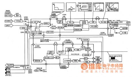
The AN33215 brightness signal processing integrated circuit is produced by the Panasonic company that can be used in the Panasonic AN-M series cameras.
1.Features
The AN33215 has the brightness signal demodulation and loss compensation processing circuit to process the replay video signal of the camera, and it bandpass filters, amplifies, limits and demodulates the replay brightness signal. The internal circuit block diagram of the AN3215S is as shown in figure 1.
Figure 1 The internal circuit block diagram and the typical application circuit of the AN3215S
2.Pin functions and data
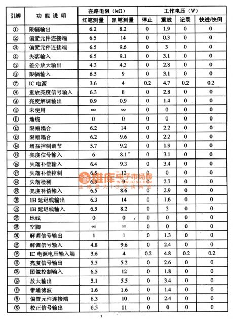
The AN3321S uses the 32-pin dual-row DIP apckage, the pin functions and data are as shown in table 1.
3.Typical application circuit
The typical application circuit of the AN3321S is as shown in figure 1.
Table 1 The pin functions and data of the AN3321S
(View)
View full Circuit Diagram | Comments | Reading(489)
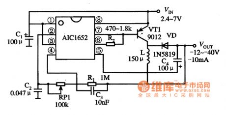
AIC1652 micro power consumption voltage reversal conversion integrated circuit
Published:2011/6/30 7:27:00 Author:Christina | Keyword: micro power consumption, voltage reversal, conversion, integrated circuit
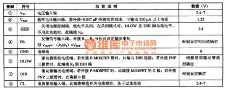
The AIC1652 micro power consumption voltage reversal conversion integrated circuit is produced by the TaiWan
Peiheng company that can be used to adjust the contrast ratio of the LCD display screen's back bias voltage,
such as the notebook type computer, the portable communication device, the portable data collection terminal products, also the negative power supply.
1.Features
The AIC1652 is composed of the reference voltage circuit, the driver circuit, the current limit current-protection circuit, the power-off control circuit and other subsidiary circuits.
2.Main electrical parameters
The input voltage range of the AIC1652 is 2.4-7V, the output voltage range is -12-40V, the output current is about -10mA, the quiescent current is about 80μA, also it has the closing mode control.
3.Pin functions and data
The AIC1652 has two kinds of packages, the AIC1652CN uses the DIP package, the AIC1652CS uses the SO package. The pin functions and data are as shown in table 1.
Table 1 The pin functions and data of the AIC1652
4.Typical application circuit
The Typical application circuit of the AIC1652 is as shown in figure 1
(View)
View full Circuit Diagram | Comments | Reading(1121)
Temperature regulation circuit diagram used in valve control
Published:2011/6/18 10:04:00 Author:Nancy | Keyword: temperature regulation, valve control

Main technical data:operating voltage: 18Vtemperature range: 25 to 95 ℃sensor maximum allwable temperature: 100 ℃temperature bias under ±10% power supply fluctuation: <0.1°Kadjustable static area: 0.2 to 1°K (View)
View full Circuit Diagram | Comments | Reading(897)
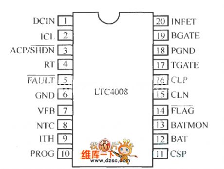
LTC4008 internal structure and external components connection circuit
Published:2011/6/30 19:38:00 Author:TaoXi | Keyword: internal structure, external components, connection circuit
View full Circuit Diagram | Comments | Reading(464)
AC voltage level circuit
Published:2011/6/30 19:47:00 Author:TaoXi | Keyword: AC, voltage level
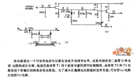
This circuit automatically or manually adjusts the level through a variable capacitor bleeder. Here the bleeder is composed of the varactor D, the capacitance and the resistance. The field effect transistor T1 can be used in the isolation between the signal source and the adjusting loop. The transistor T2 and T3 can be used to make the output circuit to has low resistance value. In order to reduce the waveform distortion when the high-frequency voltage is high, you can connect the circuit of figure (b) after the circuit of figure (a).
(View)
View full Circuit Diagram | Comments | Reading(471)
Smart phone charger module circuit
Published:2011/6/30 20:02:00 Author:TaoXi | Keyword: Smart phone, charger, module circuit
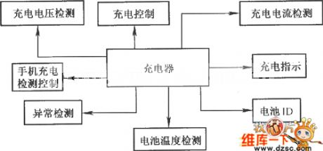
View full Circuit Diagram | Comments | Reading(490)
| Pages:390/471 At 20381382383384385386387388389390391392393394395396397398399400Under 20 |
Circuit Categories
power supply circuit
Amplifier Circuit
Basic Circuit
LED and Light Circuit
Sensor Circuit
Signal Processing
Electrical Equipment Circuit
Control Circuit
Remote Control Circuit
A/D-D/A Converter Circuit
Audio Circuit
Measuring and Test Circuit
Communication Circuit
Computer-Related Circuit
555 Circuit
Automotive Circuit
Repairing Circuit