
Index 393
Robot monitoring circuit
Published:2011/6/21 6:06:00 Author:Lucas | Keyword: Robot , monitoring circuit
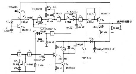
In the circuit, VT5 is the input circuit, which uses the TPSA6O3A phototransistor, and the current in VT5 can change with varying degrees of light and shade in environment. If VT5 connected the emitter resistance, the sensitivity of VT5 detecting light changes is reduced. To this, the circuit is connected the VTl transistor, and the potential of A point becomes the sum of VTl base - emitter and VD1 forward voltage drop. Usually, the current of VT5 is very low, and A point potential is almost constant. F1, F2 and VT2 and VT3, etc. constitute the motor control circuit, and Fl and F2 form the oscillator circuit.
(View)
View full Circuit Diagram | Comments | Reading(496)
The Buick-Century power window, chair, auto rearview mirror circuit
Published:2011/6/28 20:15:00 Author:qqtang | Keyword: Buick-Century, window, rearview mirror circuit
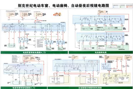
The Buick-Century power window, chair, auto rearview mirror circuit is shown in the figure.
(View)
View full Circuit Diagram | Comments | Reading(695)
Robot tracking circuit
Published:2011/6/21 5:59:00 Author:Lucas | Keyword: Robot, tracking circuit
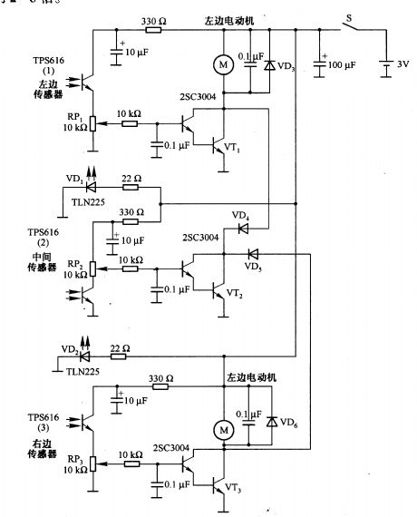
In the ircuit, TPS616 (1), TPS616 (2) and TPS616 (3) are respectively the left, middle and right light receiving sensor, which are the filter phototransistors with visible light cut-off filter. If the sensitivity of TPS616 is not enough, it can use TPS6ll. The 9OOnm peak wavelength of TPS6l1 is the same with TPS616. TLN225 is the infrared light-emitting diode with the peak wavelength in 870nm. It can also use TLNlO5 with the the peak wavelength in 950nm. Motor drive uses 2SC3004 Darlington transistor, which can also be replaced by the same type Darlington power transistor.
(View)
View full Circuit Diagram | Comments | Reading(604)
The switching output circuit of ultrasonic oscillator
Published:2011/6/21 6:33:00 Author:Lucas | Keyword: switching , output circuit , ultrasonic oscillator
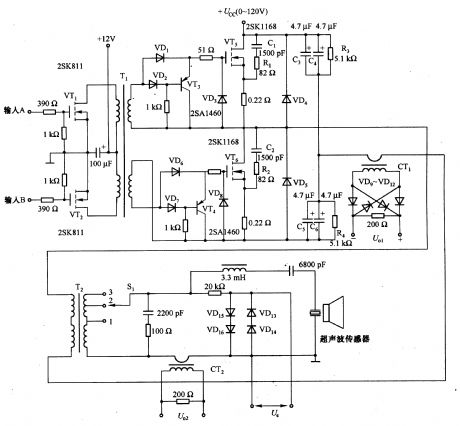
The power + U of output circuit is the DC voltage which is rectified, smoothed form the AC power. The control circuit uses +12 V power supply, therefore, it uses of transformer Tl to make the electrical isolation between low and high voltage. The inputs A and B of control circuit is the pulse voltage which is from the the 180 ° phase difference of integrated controller output, then the voltage amplified by VT1 and VT2 to drive MOSFET tubes VT5 and VT6 by passing transformer Ti. The duty cycle of VT5 and VT6 gate drive signal is approximately 45%, and the peak of gate voltage U (GS) is about lOv.
(View)
View full Circuit Diagram | Comments | Reading(631)
Broadband linear detector circuit
Published:2011/6/20 8:43:00 Author:Lucas | Keyword: Broadband , linear, detector circuit
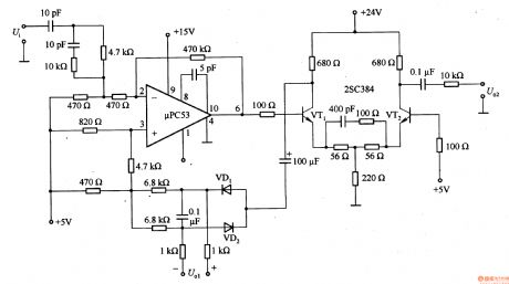
Broadband linear detector circuit is shown as the chart 1-27. It is used in the millvoltmeter and other linear detector circuits with the bandwidth in 10MHz. Uol output is the DC signal, and Uo2 output is the monitor signal. μPC53 is the broadband operational amplifier, and the output is amplified by the differential amplifier composed of VTl and VT2. The differential amplifier requires a higher supply voltage (+24 V). VD1 and VD2 are the the detector diodes, which are connected in the negative feedback circuit.
(View)
View full Circuit Diagram | Comments | Reading(1049)
Dual wave linear detector circuit
Published:2011/6/20 8:37:00 Author:Lucas | Keyword: Dual wave , linear, detector circuit
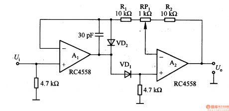
Dual wave linear detector circuit is shown as the chart. In the circuit, Ui is the AC input signal, and U is the rectifier output signal. In the positive half-cycle of AC input, A1's output is positive. As VD1 knife is positive bias, A2's input is positive, and its output is also positive, and it makes a feedback on A1 by R2, RPl and Rl, so A2 becomes a noninverting amplifier with the gain in 1; in the negative half-cycle of AC input, Al's output is also negative, and VD1 is anti-bias, then A2's inverting input is 0, that is, the working status of the inverting amplifier.
(View)
View full Circuit Diagram | Comments | Reading(547)
MC1468 regulator, main features and pin of DC-DC circuit and power supply monitor
Published:2011/6/22 6:37:00 Author:Lucas | Keyword: regulator, main features , pin , DC-DC circuit , power supply monitor
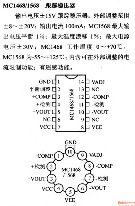
MV1468/1568 tracking regulator Their output voltage is ± 15V ; external adjustment range is ± 8 ~ ± 20V; output current is 100mA; the maximum output voltage balance of MC1568 is 1%; maximum temperature drift is 1%; maximum supply voltage is ± 30V ; MC1468 Operating Temperature is 0 ~ +70 ℃, MC1568 is -55 ~ +125 ℃; the inter includes current limiting function with the external adjustment; it has the remote control.
(View)
View full Circuit Diagram | Comments | Reading(2002)
The 6v—12v/25w DC voltage converter circuit (2)
Published:2011/6/28 21:44:00 Author:qqtang | Keyword: DC, voltage converter

Figure:The 6v—12v/25w DC voltage converter circuit (2) (View)
View full Circuit Diagram | Comments | Reading(1835)
Fixed bias circuit
Published:2011/6/28 1:41:00 Author:Christina | Keyword: Fixed, bias circuit

The fixed bias circuit is as shown in the figure, it is the common-emitter amplifier circuit. When the Ec and RB are confirmed, you can get the fixed base current and the collector current IC, so this kind of circuit is called the fixed bias circuit.
The parameters of this circuit such as the Ec, Ic, Rc, β and ICEO are generally pre-determined according to the requirements. We can use the formulas to calculate the base current (bias current) IB and the base resistance (bias resistance) RB:
IB=EC-UBE/RB≈EC/RB
IC=βIB+ICEO
We can calculate the values of IB and RB by the formulas. But in practical applications, we need to adjust the RB to get the accurate IC.
Figure: The Fixed bias circuit
(View)
View full Circuit Diagram | Comments | Reading(1315)
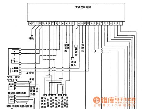
Air-conditioning control system component position circuit
Published:2011/6/28 1:43:00 Author:Christina | Keyword: Air-conditioning, control system, component position
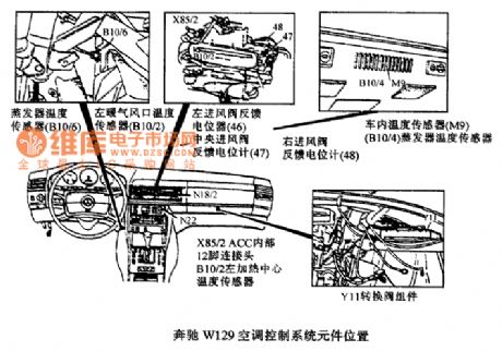
The Air-conditioning control system component position circuit:
(View)
View full Circuit Diagram | Comments | Reading(445)
Air conditioning control panel circuit
Published:2011/6/28 1:44:00 Author:Christina | Keyword: Air conditioning, control panel circuit
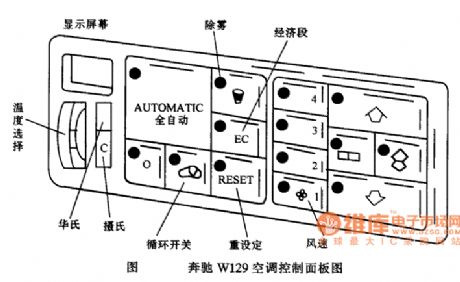
The Air conditioning control panel circuit
(View)
View full Circuit Diagram | Comments | Reading(610)
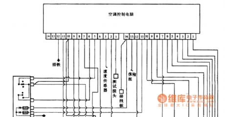
BENZ 420CE/560SEL air conditioning circuit
Published:2011/6/28 1:48:00 Author:Christina | Keyword: BENZ, air conditioning circuit
BENZ 420CE/560SEL air conditioning circuit
(View)
View full Circuit Diagram | Comments | Reading(1457)
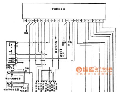
BENZ 300CE/300E/300TE air conditioning circuit
Published:2011/6/28 1:49:00 Author:Christina | Keyword: BENZ, air conditioning circuit
BENZ 300CE/300E/300TE air conditioning circuit
(View)
View full Circuit Diagram | Comments | Reading(349)
BENZ 300SE/300SEL air conditioning circuit
Published:2011/6/28 1:49:00 Author:Christina | Keyword: BENZ, air conditioning circuit
BENZ 300SE/300SEL air conditioning circuit
(View)
View full Circuit Diagram | Comments | Reading(446)
Benz W126 air-conditioning fault code timer circuit
Published:2011/6/28 1:52:00 Author:Christina | Keyword: Benz, air-conditioning, fault code, timer circuit
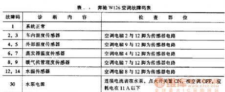
View full Circuit Diagram | Comments | Reading(430)
Benz crossover LED light circuit
Published:2011/6/28 1:58:00 Author:Christina | Keyword: Benz, crossover, LED, light circuit
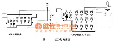
Benz crossover LED light circuit
(View)
View full Circuit Diagram | Comments | Reading(385)
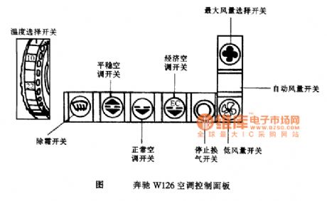
Benz W126 air conditioning control panel circuit
Published:2011/6/28 1:59:00 Author:Christina | Keyword: Benz, air conditioning, control panel
View full Circuit Diagram | Comments | Reading(1105)
38-pin diagnosis connector reading wiring circuit
Published:2011/6/28 2:03:00 Author:Christina | Keyword: 38-pin, diagnosis connector, reading wiring circuit
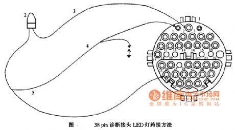
View full Circuit Diagram | Comments | Reading(486)
Columnar lithium chloride humidity sensitive resistor structure circuit
Published:2011/6/28 2:20:00 Author:Christina | Keyword: Columnar, lithium chloride, humidity sensitive resistor, structure circuit
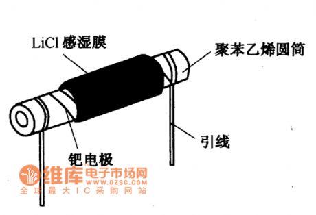
The columnar lithium chloride humidity sensitive resistor structure circuit is as shown in the figure. You can wind two parallel palladium leads on the polystyrene cylinder as the electrodes, then you can besmear the alkalization treatment lithium chloride solution on the polystyrene cylinder. Because the humidity sensing membrane can adsorb or release the water molecules to change the resistance value, so we can get the humidity value by detecting the resistance value between the electrodes.
Figure:Columnar lithium chloride humidity sensitive resistor structure circuit (View)
View full Circuit Diagram | Comments | Reading(681)
Long delay circuit 1
Published:2011/6/19 19:26:00 Author:TaoXi | Keyword: Long delay
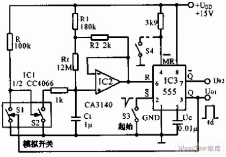
The long delay circuit is as shown in the figure, this circuit uses the 555 as the core, the high impedance op-amp CA3140 can be used as the buffer amplifier (BA), this circuit uses the bootstrapping circuit to make the charging current to maintain constant and the linearity of the charging voltage, and also the accuracy of the timing. When the pin-3 of 555 has the high electrical level, the S1 which is one of the four analog switch CC4066 conducts, the S2 cuts off, the timing capacitance C1 is charged through the R1 and Rt, the bootstrapping circuit ensures the unchanging of the R1's voltage and the charging current IC (about 10nA). So the delay time I=2UDD/3Ic=104S. S4 is the forced reset switch.
(View)
View full Circuit Diagram | Comments | Reading(583)
| Pages:393/471 At 20381382383384385386387388389390391392393394395396397398399400Under 20 |
Circuit Categories
power supply circuit
Amplifier Circuit
Basic Circuit
LED and Light Circuit
Sensor Circuit
Signal Processing
Electrical Equipment Circuit
Control Circuit
Remote Control Circuit
A/D-D/A Converter Circuit
Audio Circuit
Measuring and Test Circuit
Communication Circuit
Computer-Related Circuit
555 Circuit
Automotive Circuit
Repairing Circuit