Basic Circuit
Long delay circuit 1
Published:2011/6/19 19:26:00 Author:TaoXi | Keyword: Long delay | From:SeekIC

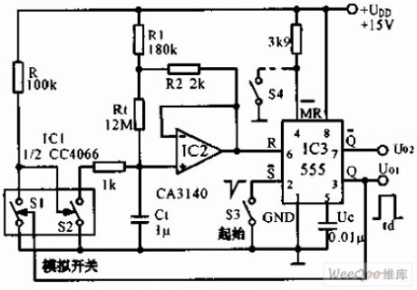
The long delay circuit is as shown in the figure, this circuit uses the 555 as the core, the high impedance op-amp CA3140 can be used as the buffer amplifier (BA), this circuit uses the bootstrapping circuit to make the charging current to maintain constant and the linearity of the charging voltage, and also the accuracy of the timing. When the pin-3 of 555 has the high electrical level, the S1 which is one of the four analog switch CC4066 conducts, the S2 cuts off, the timing capacitance C1 is charged through the R1 and Rt, the bootstrapping circuit ensures the unchanging of the R1's voltage and the charging current IC (about 10nA). So the delay time I=2UDD/3Ic=104S. S4 is the forced reset switch.
Reprinted Url Of This Article:
http://www.seekic.com/circuit_diagram/Basic_Circuit/Long_delay_circuit_1.html
Print this Page | Comments | Reading(3)

Article Categories
power supply circuit
Amplifier Circuit
Basic Circuit
LED and Light Circuit
Sensor Circuit
Signal Processing
Electrical Equipment Circuit
Control Circuit
Remote Control Circuit
A/D-D/A Converter Circuit
Audio Circuit
Measuring and Test Circuit
Communication Circuit
Computer-Related Circuit
555 Circuit
Automotive Circuit
Repairing Circuit
Code: