
Index 394
Simple gradually dark/light switch circuit (1)
Published:2011/6/27 22:22:00 Author:Ecco | Keyword: Simple , gradually dark, light, switch circuit

Usually the switch S is in the open state, and transistors VT1, VT2 are turned off, then light E is off. Just close the S, 220V AC is rectified by the VD1 ~ VD4 and becomes pulsating DC output, which will charge for capacitor C through switch S and resistor R, so the voltage across C is gradually increased. Thus VT1 can obtain the base bias from low to high by R2, then VT1, VT2 enter the enlarged state gradually from deadline state, finally into a fully on state, so the light E is brighten from dark gradually.
(View)
View full Circuit Diagram | Comments | Reading(823)
Voltage monitor circuit
Published:2011/6/27 4:27:00 Author:Ecco | Keyword: Voltage , monitor circuit
View full Circuit Diagram | Comments | Reading(549)
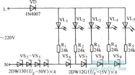
Photoelectric photometry switch circuit diagram
Published:2011/6/27 4:56:00 Author:Ecco | Keyword: Photoelectric, photometry, switch
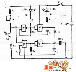
After the power switch K is turned on, beat pulse generator and audio oscillator pulse will begin to work. In the part of beat pulse generator, YF1 and YF2 output pulses have opposite polarity. With the output of oscillator pulse, light emitting diodes LED1 and LED2 alternately emit light, and the flash cycle is determined by R3, C1 values; in the part of audio oscillator, the oscillation voltage is determined by the output end of YF4, then HTD issues single-frequency sound, and the audio pulse frequency is established by the R7, C2 values.
(View)
View full Circuit Diagram | Comments | Reading(452)
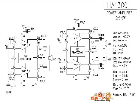
HA13001 audio IC circuit diagram
Published:2011/6/27 5:12:00 Author:Ecco | Keyword: audio, IC circuit
View full Circuit Diagram | Comments | Reading(2250)
The typical application circuit diagram of nRF401
Published:2011/6/27 5:12:00 Author:Ecco | Keyword: typical application
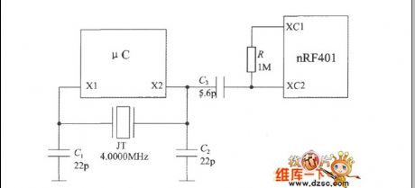
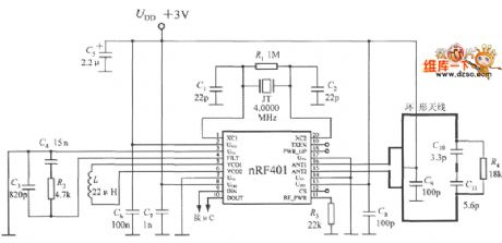
UDD uses +3 V supply. The R1, JT, C1 and C2 constitute the crystal circuit, and C3, C4 and R2 form the loop filter. R3 is the power set resistor. C5 is the power supply decoupling capacitor; C6 and C7 are noise reduction capacitors. DIN, DOUT terminals are respectively connected MCU TXD (serial output), RXD (serial input) sides. To simplify the circuit, nRF401 μC can be combined with a crystal oscillator circuit, the circuit is shown as below. X1, X2 are respectively μC crystal input end and output end, the resulting crystal frequency is directly sent to the XC2 side of nRF401.
(View)
View full Circuit Diagram | Comments | Reading(465)
Text displaying logic pen 4 circuit diagram composed of gate circuit
Published:2011/6/27 3:55:00 Author:Ecco | Keyword: Text, displaying , logic pen , gate circuit
View full Circuit Diagram | Comments | Reading(427)
Time-scale circuit and the programmable frequency divider circuit
Published:2011/6/20 1:53:00 Author:TaoXi | Keyword: Time-scale, programmable, frequency divider
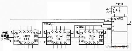

Time-scale circuit
The sequence signal generator:
Design steps: the first step is to form a model P counter; the second step is to select the appropriate data selector. You need to add the sequence which you want to produce to the data input port of the data selector in specified order, and you also need to connect the address port with the output port of the counter, the output port of the data selector will produce the sequence signal.
The programmable frequency divider: the counter can divide the frequency of the count pulse, and you can change the frequency dividing ratio by changing the mode of the counter. According to the principle, we can use the integrated counter to form the frequency divider that has the changeable frequency dividing ratio, it is the programmable frequency divider.
(View)
View full Circuit Diagram | Comments | Reading(3234)
Mode-6 counter circuit composed of the reset port and the preset port
Published:2011/6/20 1:58:00 Author:TaoXi | Keyword: Mode-6 counter, reset port, preset port
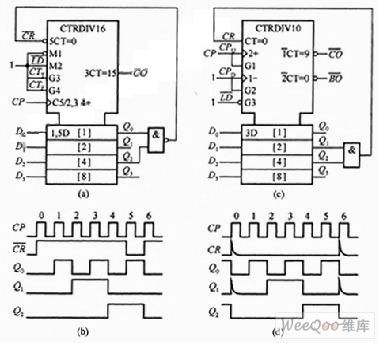
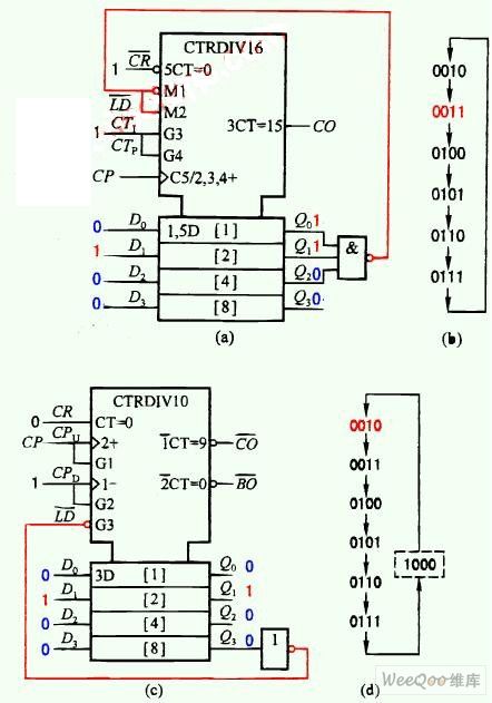
By using the reset port and the preset port of the counter, we can form the any-mode counter.
The figure shows the mode-6 counters which are composed of the 74163 and 74192, the operating waveform is as shown in the figure.
The mode-6 counter which is composed of the preset port (View)
View full Circuit Diagram | Comments | Reading(1534)
TA7668 integrated circuit with dual channels preposing of recording,playback
Published:2011/6/17 20:58:00 Author:chopper | Keyword: integrated circuit, dual channels, preposing, recording, playback

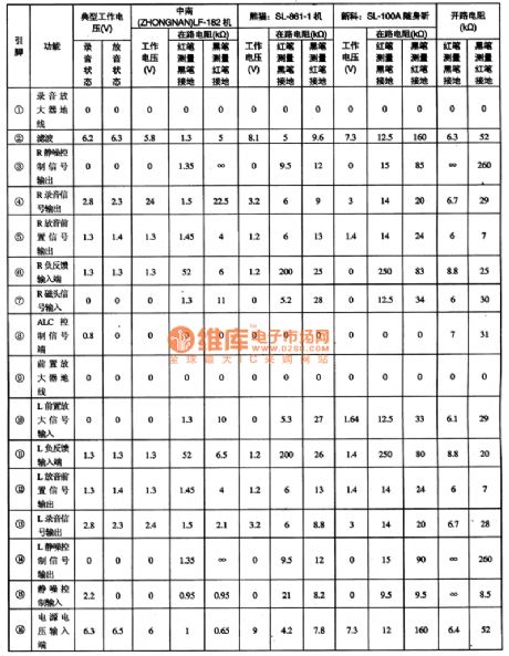
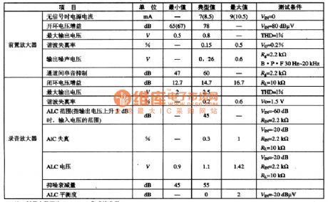
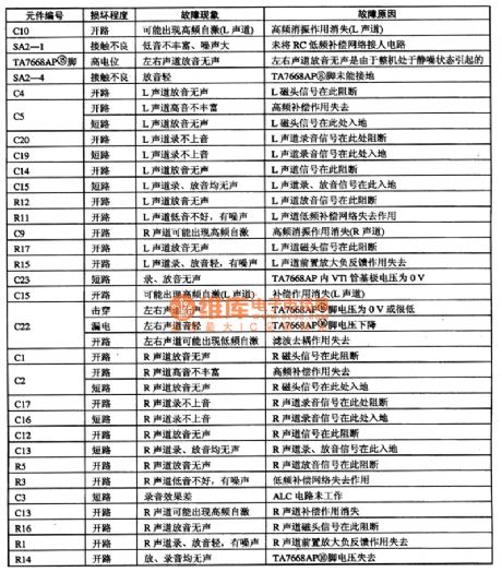
TA7668 is a typical integrated circuit with dual channels preposing of recording,playback.This IC is applied to sound system like walkman,radio-tape recorder,music center widely.1.the inner circuit and typical application of TA7668The inner circuit and typical application of TA7668 integrated package are shown as picture 1.The amplifiers of the record circuit are independent.IC includes automatic level control,noise elimination and other functional circuits besides two preamplifiers of same function and recording post-amplifier.
(View)
View full Circuit Diagram | Comments | Reading(2247)
ADC0809 interface circuit
Published:2011/6/20 3:23:00 Author:TaoXi | Keyword: interface circuit
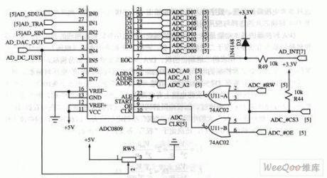
ADC0809 interface circuit (View)
View full Circuit Diagram | Comments | Reading(1173)
TA7373F stereo demodulation integrated circuit
Published:2011/6/16 0:54:00 Author:chopper | Keyword: stereo, demodulation, integrated circuit
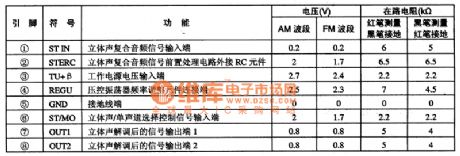
TA7373F is a stereo demodulation integrated circuit produced by Company TOSHIBA and it is applied to sound systems such as voltage walkman as FM stereo signal demodulation.1.function characteristicsTA7373F integrated circuit includes stereo signal demodulation circuit,stereo/monophony selection control circuit,stereo demodulation preamplifier circuit,frequency dividing circuit,and other miscellaneous function circuits.2.Function and data of pinsTA7373F adopts 8 pins dual inline package.And its function and data of pins of the integrated circuitare shown as chart 1.
(View)
View full Circuit Diagram | Comments | Reading(493)
Filter circuit can be used in the IF amplifier
Published:2011/6/23 21:41:00 Author:TaoXi | Keyword: Filter circuit, IF amplifier
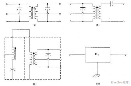
The function of the IF amplifier is to supply the gain and the selectivity for the receiver, the selectivity part is realized by different filters. The filters that can be used in the IF amplifier are as shown in the figure. The typical application circuit is as shown in figure (a), the transformer of the figure has the tapping, but the non-tapping transformer also can be used. The tapping can supply the low impedance connection and keep the advantage of the high-impedance tuning circuit. You should notice that the capacitance is usually in the transformer isolation cover.
Most of the specialized superheterodyne radio receiver's gain and selectivity are supplied by the intermediate frequency (IF) amplifier, so it is a high-gain narrow-bandwidth amplifier.
Figure: All kinds of intermediate frequency filter circuits (View)
View full Circuit Diagram | Comments | Reading(458)
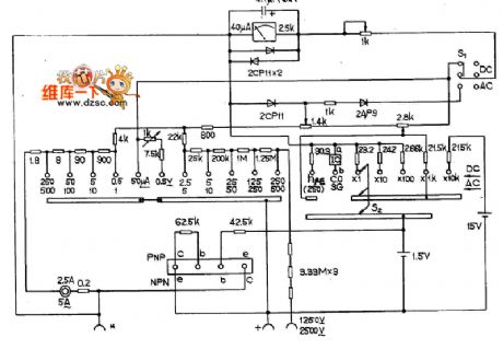
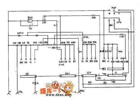
MF107 multimeter circuit diagram
Published:2011/6/24 4:44:00 Author:Nicole | Keyword: multimeter
View full Circuit Diagram | Comments | Reading(854)
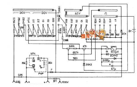
MF125 multimeter circuit diagram
Published:2011/6/24 4:44:00 Author:Nicole | Keyword: multimeter
View full Circuit Diagram | Comments | Reading(532)
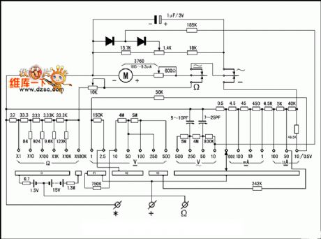
MF368 multimeter circuit diagram
Published:2011/6/24 4:43:00 Author:Nicole | Keyword: multimeter
View full Circuit Diagram | Comments | Reading(777)
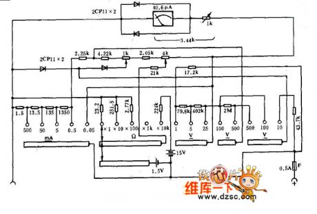
MF-10 multimeter circuit diagram
Published:2011/6/24 4:43:00 Author:Nicole | Keyword: multimeter
View full Circuit Diagram | Comments | Reading(1361)
MF30 multimeter circuit diagram
Published:2011/6/24 4:43:00 Author:Nicole | Keyword: multimeter
View full Circuit Diagram | Comments | Reading(624)
Multistage communication filter circuit
Published:2011/6/23 21:48:00 Author:TaoXi | Keyword: Multistage, communication, filter circuit
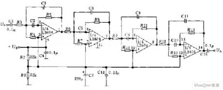
The filter circuit is as shown in the figure, the center frequency fc=1.180Hz, the gain Kv=1,C2=C3=C5=C6=C8.
(View)
View full Circuit Diagram | Comments | Reading(447)
Active dual two-stage bandpass filter circuit
Published:2011/6/23 21:51:00 Author:TaoXi | Keyword: Active, dual, two-stage, bandpass filter
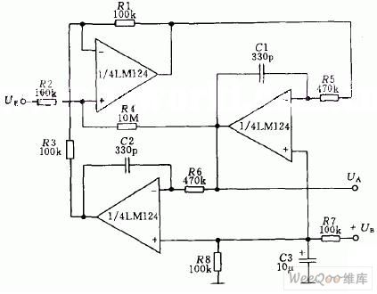
The active dual two-stage bandpass filter circuit is as shown in the figure, the center frequency is 1kHz, the quality factor Q=50, the gain Kv=100 (equivalent to 40 dB).
(View)
View full Circuit Diagram | Comments | Reading(753)
Frequency adjustable bandpass filter circuit
Published:2011/6/23 22:05:00 Author:TaoXi | Keyword: Frequency adjustable, bandpass, filter
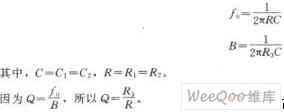
The frequency adjustable bandpass filter circuit is as shown in the figure. This filter's resonance frequency can be adjusted through the coaxial potentiometer, and the Q value will not change when you are adjusting the frequency. The Q value of the active band-pass filter of the figure is about 30, the resonant frequency can be changed from 150Hz to 1.5kHz, in this range the changing range of Q is less than 5%. For ease of the calculation, you need to set the potentiometer to the top, the resonant frequency f0 and the bandwidth B are:
Changing the position of the potentiometer is equivalent to add a voltage divider, so the current of R1, R2 and R3 reduce.
(View)
View full Circuit Diagram | Comments | Reading(2019)
| Pages:394/471 At 20381382383384385386387388389390391392393394395396397398399400Under 20 |
Circuit Categories
power supply circuit
Amplifier Circuit
Basic Circuit
LED and Light Circuit
Sensor Circuit
Signal Processing
Electrical Equipment Circuit
Control Circuit
Remote Control Circuit
A/D-D/A Converter Circuit
Audio Circuit
Measuring and Test Circuit
Communication Circuit
Computer-Related Circuit
555 Circuit
Automotive Circuit
Repairing Circuit