
Index 386
Byd MOS Tube Supply
Published:2011/6/24 10:09:00 Author:Michel | Keyword: Byd, MOS Tube, Supply

Detailed Instructions of Byd MOS Tube Supply and Mosfet
Original:BF92N60,BF94N60,BF96N60,BF98N60,BF910N60,BF912N60
Properties and advantages: stable performance and preferential price
Product use: switching power supply, adapters, HID ballast
After-sales service: We provide technical support, and the original BYD signed agreement of the quality.
Packing: tubes (each tube 50 PCS), each box 5000 PCS. The package TO 220 (F)
Note: shenzhen Aisen science and technology is the agent of BYD series
MOS,namely,BF92N60,BF94N60,BF96N60,BF98N60,BF910N60,BF912N60 and we have stocks for long time and welcome to call Mr Zhao via13760184506.In addition,our company is the agent of BYD power management IC-BF1501,AC/AC.
Welcome to download and the information is from www.dzsc.com. (View)
View full Circuit Diagram | Comments | Reading(700)
Voice Filter Circuit of LM387
Published:2011/6/24 2:12:00 Author:Michel | Keyword: Voice, Filter Circuit

Serial Voice frequency range filter circuit is shown as above and its frequency range is 360Hz-3KHz. (View)
View full Circuit Diagram | Comments | Reading(1238)
Complementary tube double bistable circuit
Published:2011/6/30 8:09:00 Author:Fiona | Keyword: Complementary tube, double bistable


Complementary tube double bistable circuit is shown in Figure 1 (a).When it is charged tothe power supply,if there is no trigger effect,because the collector current is very small and the voltage of Rc1 and Rc2 is also small,two tubes are both off,the circuit keeps the steady state.Under the trigger pulse,assume BG1 changes from close to enlarge,and produces following the avalanche of positive feedback process.Quickly make the two tubes be saturate connected,in another steady state,capacitance C1 is accelerated capacitance,by the form 1(b) visible,uc1 is steeply down to zero,but UC2 is steeply from zero up to Ec.
(View)
View full Circuit Diagram | Comments | Reading(861)
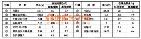
LA7846N-Vertical scanning output thick-film integrated circuit
Published:2011/6/30 15:45:00 Author:leo | Keyword: LA7846N-Vertical scanning output thick-film integrated circuit

LA7846N is vertical scanning output thick-film integrated circuit which is widely used in big screen color television.
Function features:The integrated circuit LA7846N contains field deflection urging circuit, field deflection power amplifier circuit, pump power supply circuit, protecting circuit and other related circuits.
Pin functions and data:The integrated circuit LA7846N uses 10 pin single line package. Pin functions and data are shown in the picture. (View)
View full Circuit Diagram | Comments | Reading(788)
Optical receiver circuit diagram
Published:2011/7/2 21:18:00 Author:leo | Keyword: Optical receiver circuit diagram, LA7224

The picture shows a optical receiver circuit. In this circuit, LA7224 is a kind of front amplifier which is used to receive signals. Peak value keeping circuit, integral circuit and so on can form the integrated circuit of the same chip. The syntony circuit formed by L and G2 are used to get carrier and the carrier comes through the amplitude-limited circuit to keep the peak value (C3), by which the S/N of this circuit is improved. C4 is integral circuit and capacitor recommended is 0.0047μF. When the output voltage of the pin 1 of LA7224 is 0.3 V, VT1 is stopped and output voltage is U which is a high value. (View)
View full Circuit Diagram | Comments | Reading(867)
LA7845N-Field scanning output integrated circuit
Published:2011/7/2 21:27:00 Author:leo | Keyword: LA7845N-Field scanning output integrated circuit

LA7845N is a kind of field scanning output integrated circuit made by Sanyo corporation which is widely used in big screen color television.
It has few peripheral components and adopts negative sources to offer the power. It does not perfect over current, overvoltage and overheating protecting circuit. Besides, the maximum output current of it is 3Ap-p and the maximum power consumption is 11W while the maximum output voltage is 40 V. The maximum source output voltage can reach 85 V. The inner circuit of this integrated circuit is shown in the picture and you can also find the pin functions and related data in it. (View)
View full Circuit Diagram | Comments | Reading(672)
LA7840, LA7841, LA7845 and LA7846-Field scanning output integrated circuit
Published:2011/7/3 2:09:00 Author:leo | Keyword: LA7840, LA7841, LA7845 and LA7846-Field scanning output integrated circuit

LA7840, LA7841, LA7845 and LA7846 are a kind of field scanning output integrated circuit made by Sanyo Corporation in Japan. They are widely used in color television with different screens.
1.Function features:
They have vertical output circuit, over current protecting circuit and use DC differential input method. The maximum output current of LA7840 is 1.8Ap-p and the maximum output power is 9W. The maximum output current of LA7841 is 2.2Ap-p and the maximum output power is 9W. The maximum output current of LA7845 is 2.2Ap-p and the maximum output power is 11W. The maximum output current of LA7846 is 3Ap-p and the maximum output power is 20W.
2.in functions and related data:
All information about their pin functions and related data are shown in the picture.
(View)
View full Circuit Diagram | Comments | Reading(4853)
LA7838-Field scanning output integrated circuit
Published:2011/7/3 2:16:00 Author:leo | Keyword: LA7838-Field scanning output integrated circuit
LA7838 is a type of field scanning output integrated circuit made by Sanyo Cooperation in Japan. It is widely used in color television.
1.Function features:
The integrated circuit LA7838 contains saw tooth generator circuit, field scanning output circuit, and other related circuits.
2.The integrated circuit LA7838 adopts 13 pin single line packages. The related information is all shown in the picture.
Reminder: LA7838 the reducing output capability of the capacitor pin 12 will cause retrace line shows in the screen. (View)
View full Circuit Diagram | Comments | Reading(520)
TMP87CS38N-XXXX-Projection VT dedicated single chip microcomputer integrated circuit
Published:2011/7/3 2:52:00 Author:leo | Keyword: TMP87CS38N-XXXX-Projection VT dedicated single chip microcomputer integrated circuit

(View)
View full Circuit Diagram | Comments | Reading(719)
TMP87CS38N-Single chip microcomputer integrated circuit
Published:2011/7/3 3:08:00 Author:leo | Keyword: TMP87CS38N-Single chip microcomputer integrated circuit

TMP87CS38N is a kind of single chip microcomputer integrated circuit made by Toshiba in Japan. It is especially used in the microcontroller chip of changhong projection color television 51PT28A.
1.Function features:The integrated circuit TMP87CS38N, memory AT25C08, IR-Control emitter K8G, IR-Control signal receiver HSO038 as well as interface circuits form complete color television remote control circuit. Except the various control functions, it has +148 V, +18 V and -18 V power supply over current test and protection function.
2.Pin functions and related data:The integrated circuit TMP87CS38N adopts 42 pin dual line package. All information is shown in the picture. (View)
View full Circuit Diagram | Comments | Reading(635)
MG45 & MG44 resin package circuit
Published:2011/7/4 20:21:00 Author:Christina | Keyword: resin package

View full Circuit Diagram | Comments | Reading(976)
Structure circuit of the photosensitive diode
Published:2011/7/3 22:16:00 Author:Christina | Keyword: Structure circuit, photosensitive diode
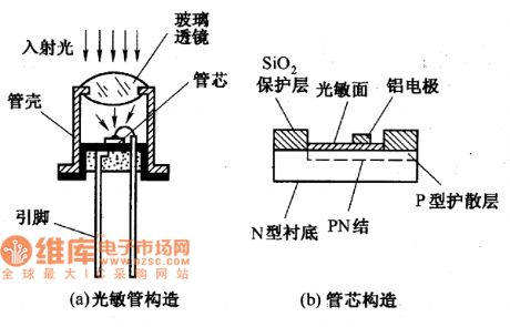
The photosensitive diode is also called photoelectric diode, it has the same structure with the general semiconductor diode. The figure shows the structure of the photosensitive diode. There is a glass lens on the photodiode shell, the incident light is shining on the tube core through the glass lens. The tube core of the light-emitting diode is the PN junction with the photosensitive properties, it is packaged in the tube shell. The photosensitive surface of the light-emitting diode is the film of the N-type silicon. The PN junction of the light-emitting diode's core and the core itself have large area, but the electrode area of the tube core is small.
(View)
View full Circuit Diagram | Comments | Reading(923)
BENZ 190 series ABS system circuit
Published:2011/7/4 3:44:00 Author:Christina | Keyword: BENZ, ABS, system circuit
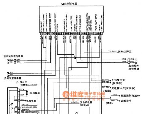
BENZ 190 series ABS system circuit (View)
View full Circuit Diagram | Comments | Reading(606)
Transistor radio application circuit of the ceramic filter
Published:2011/7/4 1:38:00 Author:Christina | Keyword: Transistor radio, application circuit, ceramic filter
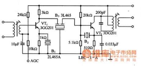
The transistor radio application circuit of the two-port and three-port ceramic filter. The ceramic filters B1 and B2 can be used in the 465kHz intermediate frequency bypass, the B1 can be used in the coupling of the intermediate frequency. B1 uses the narrowband type filter, and it is connected with the emitter resistance of the VT1, this design helps to eliminate the interference and noise.
Figure 1 The transistor radio application circuit of the ceramic filter
(View)
View full Circuit Diagram | Comments | Reading(1491)
MG type photosensitive resistor dimension circuit
Published:2011/7/4 19:36:00 Author:Christina | Keyword: MG type, photosensitive resistor, dimension circuit
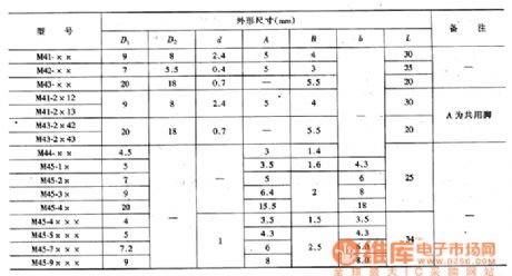
Table: MG type photosensitive resistor dimensions (View)
View full Circuit Diagram | Comments | Reading(535)
Unijunction crystal thyristor trigger circuit
Published:2011/7/4 19:21:00 Author:Christina | Keyword: Unijunction crystal, thyristor, trigger

The thyristor trigger circuit is as shown in figure 1. The unijunction crystal thyristor forms the self-excited multivibrator, the series pulse current which is produced by it flows through the pulse transformer T, so the secondary stage of the transformer T will produce a series of pulse voltage, the VD1 cuts the negative pulse of this series pulse and this pulse adds to the triggered thyristors VS between the control electrode and the cathode.
The pulse transformer of this circuit can be used to trigger the pulse generating circuit and isolate the thyristor main circuit.
Figure 1 The thyristor trigger circuit
(View)
View full Circuit Diagram | Comments | Reading(1321)
Powerhope UPS battery cannot charging maintenance circuit diagram
Published:2011/6/24 2:29:00 Author:Ecco | Keyword: Powerhope , UPS battery , cannot charging, maintenance
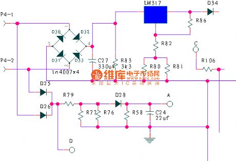
Repairing parts: 1. good or bad of four diodes D30, D31, D32, D33 in bridge rectifier; 2. leakage of filter capacitor C27 ; 3. good or bad of LM317; 4.LM317 external resistors R83, R80, R81, R82, R83, R86 is changing value or not; 5 charging diode D34 is good or bad.
(View)
View full Circuit Diagram | Comments | Reading(2243)
16-pin diagnosis connector reading wiring circuit
Published:2011/7/4 1:56:00 Author:Christina | Keyword: 16-pin, diagnosis connector, reading, wiring circuit
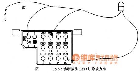
The 16-pin diagnosis connector reading wiring circuit
(View)
View full Circuit Diagram | Comments | Reading(605)
Polaris JD-11W electronic ballast circuit diagram
Published:2011/6/30 22:37:00 Author:Ecco | Keyword: Polaris , electronic ballast

View full Circuit Diagram | Comments | Reading(1798)
Transistor switching circuit diagram
Published:2011/6/30 3:08:00 Author:Ecco | Keyword: Transistor, switching
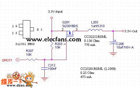
In the Figure: when GPIO end is low, the transistor turns on, then the pin 3 output is 3. 3V; when GPIO terminal is high, the transistor is off, the pin 3 output is 0V.
(View)
View full Circuit Diagram | Comments | Reading(681)
| Pages:386/471 At 20381382383384385386387388389390391392393394395396397398399400Under 20 |
Circuit Categories
power supply circuit
Amplifier Circuit
Basic Circuit
LED and Light Circuit
Sensor Circuit
Signal Processing
Electrical Equipment Circuit
Control Circuit
Remote Control Circuit
A/D-D/A Converter Circuit
Audio Circuit
Measuring and Test Circuit
Communication Circuit
Computer-Related Circuit
555 Circuit
Automotive Circuit
Repairing Circuit