
Index 395
High Q value trapped wave filter circuit
Published:2011/6/23 22:19:00 Author:TaoXi | Keyword: High Q value, trapped wave, filter circuit
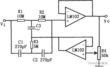
The high Q value trapped wave filter circuit is as shown in the figure. Because the double-T network filter can have the better attenuation characteristics only when it is far away from the resonance frequency f0, so the Q value of the filter is not high. If the output signal of the filter is output by the voltage output device (the gain is 1), and it is feedback to the double-T network to form the bootstrap, so when the input signal attenuates for 0.3, the Q value is more than 50. The voltage follower is composed of the op-amp, the potentiometer R4 can continuously change the Q value of the circuit (from 0.3 to 50), the trapped wave frequency f0=1/2πR1C1.
(View)
View full Circuit Diagram | Comments | Reading(579)
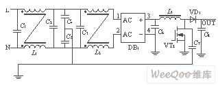
DC voltage stabilization power supply LC filter circuit
Published:2011/6/23 21:54:00 Author:TaoXi | Keyword: DC, voltage stabilization, power supply, LC, filter circuit
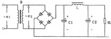
DC voltage stabilization power supply LC filter circuit (View)
View full Circuit Diagram | Comments | Reading(4048)
Narrow-band filter circuit with the adjustable Q value and frequency
Published:2011/6/23 22:28:00 Author:TaoXi | Keyword: Narrow-band, filter circuit, adjustable, Q value, frequency
The narrow-band filter circuit with the adjustable Q value and frequency is as shown in the figure. This circuit is an active narrowband filter with adjustable Q value and frequency. It uses the Venturi bridge positive feedback, the loop gain is lower than 1. The feature of this circuit is if you adjust the Q value, you will not influence the center frequency. Because the Q value only has relationship with the gain of the return circuit. When the gain is 600, the Q value is 2000; when the gain is 140, the Q value is 30. In general venturi bridge oscillators, for the in-phase input ports, the amplifier gain must be more than 3 to start oscillation, the amplifier gain is less than 3 in this circuit.
(View)
View full Circuit Diagram | Comments | Reading(836)
Trapped wave filter circuit uses the operational amplifier as the voltage follower
Published:2011/6/23 22:34:00 Author:TaoXi | Keyword: Trapped wave, filter circuit, operational amplifier, voltage follower
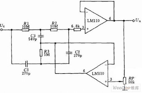
The trapped wave filter circuit which uses the operational amplifier (composed of two LM110 or SN72310) as the voltage follower is as shown in the figure.
(View)
View full Circuit Diagram | Comments | Reading(493)
The filter circuit of the output return circuit
Published:2011/6/22 2:35:00 Author:TaoXi | Keyword: filter circuit, output return circuit
In the frequency range of 0.15~1MHz, the harassment mainly exists in the form of common mode, in the frequency range of 1~10MHz, the harassment mainly exists in the forms of differential mode and common mode, when the frequency range is higher than 10MHz, the harassment mainly exists in the form of common mode. The differential mode harassment is caused by the switch tube that is in the operating state, when the switch tube opens, the current of the power line rises linearly, when the switch tube closes, the current is zero, so the current of the power line is the high frequency triangle pulse current, and it has rich high-frequency harmonic component.
(View)
View full Circuit Diagram | Comments | Reading(384)
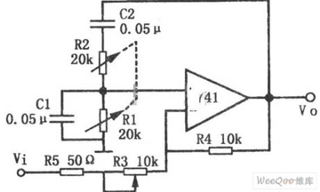
Single peak feature filter circuit
Published:2011/6/22 2:34:00 Author:TaoXi | Keyword: Single peak, feature, filter circuit

The single peak feature filter circuit which is composed of the single op-amp is as shown in the figure. This circuit uses a op-amp and a few components to form the filter, it has the same features with the filter circuit that is composed of the LC components, if you do not change the circuit gain, you can adjust the resonant frequency easily. This circuit uses the potentiometer PR1 to adjust the resonance frequency. When the value of PR1 is from the maximum to the minimun, the resonance frequency adjustment range is:
(View)
View full Circuit Diagram | Comments | Reading(485)
Single-phase full wave rectifier filter circuit
Published:2011/6/22 2:36:00 Author:TaoXi | Keyword: Single-phase, full wave, rectifier, filter
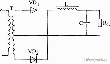
Single-phase full wave rectifier filter circuit (View)
View full Circuit Diagram | Comments | Reading(1153)
Logarithmic characteristic photosensitive circuit
Published:2011/6/22 2:39:00 Author:TaoXi | Keyword: Logarithmic characteristic, photosensitive
Logarithmic characteristic photosensitive circuit (View)
View full Circuit Diagram | Comments | Reading(441)
Double color complementation alternate display running water color light circuit
Published:2011/6/22 19:39:00 Author:TaoXi | Keyword: Double color, complementation, alternate display, running water, color light
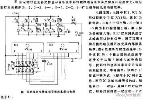
The circuit principle: in the circuit, IC1 and IC2 are the color light control special IC RY168. This IC is in the soft package, it has eight pinouts. The 2-5 pins are the color light control output port, the pin-8 is the audio input port. This IC uses the dual-channel leap mode to output the color light control signal, you can change the internal oscillation frequency by adjusting the potentiometer which is connected with the pin-6, then you can change the chase rate of the color light. In addition, the chase rate of the four output ports of this IC is controlled by the music signal which is input from pin-8. In this circuit, there are two ICs connected into parallel.
(View)
View full Circuit Diagram | Comments | Reading(462)
Hitting target sphere "wishing you prosperity" pronunciation alarm circuit diagram
Published:2011/6/23 22:40:00 Author:Nicole | Keyword: target sphere, wishing you prosperity, pronunciation alarm
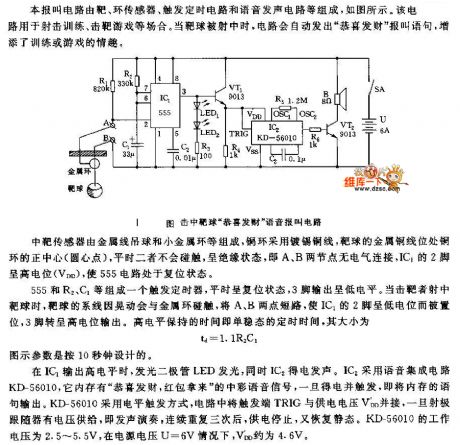
The hitting target sensor is composed of gold line drop ball and small gold loop, the copper loop adopts tinned copper wire, the target ball's gold copper wire is in the midpoint(center point)of copper ring, ordinarily, they will not touch, they are in insulation state, namely, the two points of A, B have no electricity connection, IC1's 2 foot is high level(VDD), the 555 circuit is in reset state.
A trigger timer is made of 555 and R2, C1, ordinarily, it is in reset state, 3 foot output is low level. When people hit the target, the tie line of target will touch the gold loop due to shake, then A, B points are short circuit, IC1's 2 foot is low level and it is set, 3 foot turns to high level output. The high level's hold time, namely, the monostable timing time is td=1.1R2C1.
(View)
View full Circuit Diagram | Comments | Reading(461)
Charge pump circuit
Published:2011/6/23 2:42:00 Author:TaoXi | Keyword: Charge pump

The charge pump phase locked loop has the features of low power consumption, high speed, little jitter and low cost, it can be used in the wireless communication, the frequency synthesizer and the clock recovery circuit. The charge pump circuit plays the very important role in the phase locked loop(PLL), the main function of it is to change the UP and DOWN digital signals of the PFD into the analog signal, so we can control the frequency of the voltage-controlled oscillator (VCO). When the PFD gives the high precision phase error, the charge pump plays a decisive role to the performance of the whole loop.
(View)
View full Circuit Diagram | Comments | Reading(784)
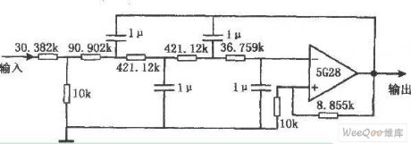
Bandwidth adjustable audio filter circuit with the 900Hz center frequency
Published:2011/6/23 21:19:00 Author:TaoXi | Keyword: Bandwidth, adjustable, audio filter, 900Hz, center frequency

This circuit uses the Wien-bridge, it has the adjustable bandwidth and the center frequency is 900Hz, if the 10K potentiometer's level is too low, there will be the circuit oscillation.
(View)
View full Circuit Diagram | Comments | Reading(774)
Bart woz fourth-stage active low-pass filter circuit
Published:2011/6/23 21:27:00 Author:TaoXi | Keyword: Bart woz, fourth-stage, active, low-pass filter
This device is designed as the Bart woz fourth-stage active low-pass filter circuit that can be used to filter the very low frequency random impulsive noise interference voltage of the DC level signal, the cut-off frequency (-3dB) is about 8Hz, the gain reduces 20dB when the frequency is 18Hz. The pass-band natural attenuation is 0.467. The input resistance is about 40kΩ. The filter network resistor is composed of some metal film precise resistance. If the 1μF capacitance has the good precision, the cut-off frequency fc closes to the theoretical value.
(View)
View full Circuit Diagram | Comments | Reading(531)
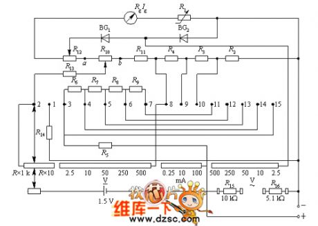
MF27-2 multimeter circuit diagram
Published:2011/6/24 4:10:00 Author:Nicole | Keyword: multimeter
View full Circuit Diagram | Comments | Reading(943)
MF28 multimeter circuit diagram
Published:2011/6/24 4:35:00 Author:Nicole | Keyword: multimeter

View full Circuit Diagram | Comments | Reading(1287)
Audi front seat heating circuit
Published:2011/6/27 3:18:00 Author:TaoXi | Keyword: Audi, front seat, heating circuit
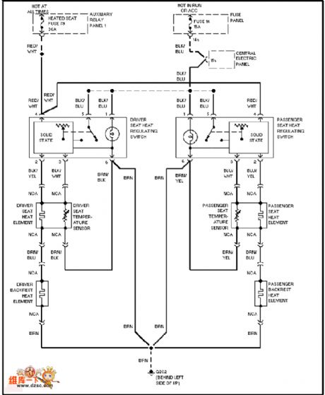
View full Circuit Diagram | Comments | Reading(513)
Single stage PFC circuit
Published:2011/6/27 3:15:00 Author:TaoXi | Keyword: Single stage, PFC
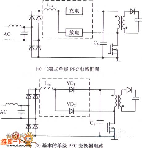
When the convertor of the electric car charger is working in the high frequency state, it will cause the harmonic pollution to the power grid, so we must do some effective actions to limit the total harmonic quantity of the electric car charger's convertor. For now, the charging converter must meet the IEEE519-1992 standard or the similar standards. To meet these standards, the charging converter can use the single stage or two stage PFC circuit and the integrated charger. To further improve the conversion efficiency, we can use the soft-switching circuit in the high frequency condition to reduce the power consumption of the switch tube.
(View)
View full Circuit Diagram | Comments | Reading(943)
Medicinal automatic timing erythrocyte sedimentation rate shelf
Published:2011/6/24 8:17:00 Author:Nicole | Keyword: automatic timing, erythrocyte sedimentation rate, shelf
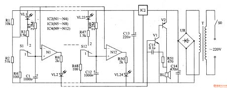
This medicinal automatic timing erythrocyte sedimentation rate shelf circuit is composed of power supply circuit, sound alarming circuit and timing circuit, it is shown in the figure 9-158.
The power supply circuit is made of power supply switch SO, power supply transformer T, rectifier quad UR, filter capacitor C13, C14 and three terminal regulator integrated circuit IC1.
The sound alarming circuit consists of transistors V1, V2, resistor R5, capacitor C13 and loudspeaker BL.
The 220V voltage is pressure released by T, it is rectificated by UR, it is filtered by C14, it is regulated voltage by IC1, one path provides IC2-IC4 with +12V work voltage, after divided voltage by R1, R2, the other path provides N1-N12's phase reversal input terminal with reference voltage.
(View)
View full Circuit Diagram | Comments | Reading(628)
Unfired bricks moisture detector 2
Published:2011/6/26 22:30:00 Author:Nicole | Keyword: Unfired brick, moisture, detector
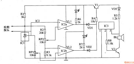
This unfired bricks detector circuit is composed of humidity detector probe, steady voltage reference voltage, comparator, switch circuit and acousto-optic alarm circuit, it is shown in the figure 8-76.
The comparator circuit is made of integrated circuit IC2 and resistors R2, R3, potentiometers RP1, RP2.
The switch circuit consists of switch tube V1, diodes VD1, VD2 and resistor R4.
The acousto-optic alarm circuit is composed of LEDs VL1, VL2, resistors R6, R7, music integrated circuit IC3, audio amplifier tube V2 and loudspeaker BL.
(View)
View full Circuit Diagram | Comments | Reading(1095)
74 series digital circuit 74LS440/441 four 3-directions bus transceiver
Published:2011/6/26 21:35:00 Author:Nicole | Keyword: 74 series, digital circuit, bus transceiver
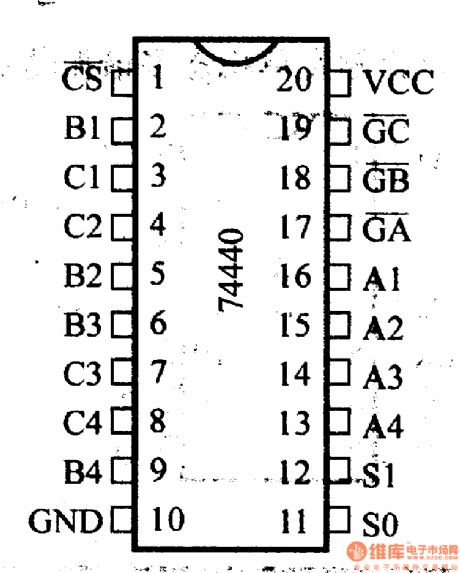

74LS440/441/442/443/444, 74HC442/443/444 four 3-directions bus transceiver
74LS440/441 is OC output, 74LS442/443/444 are there state output
The functional table
(View)
View full Circuit Diagram | Comments | Reading(690)
| Pages:395/471 At 20381382383384385386387388389390391392393394395396397398399400Under 20 |
Circuit Categories
power supply circuit
Amplifier Circuit
Basic Circuit
LED and Light Circuit
Sensor Circuit
Signal Processing
Electrical Equipment Circuit
Control Circuit
Remote Control Circuit
A/D-D/A Converter Circuit
Audio Circuit
Measuring and Test Circuit
Communication Circuit
Computer-Related Circuit
555 Circuit
Automotive Circuit
Repairing Circuit