
Automotive Circuit
Index 67
Nissan A32-EL board computer circuit
Published:2011/6/22 10:19:00 Author:Nancy | Keyword: Nissan, board computer
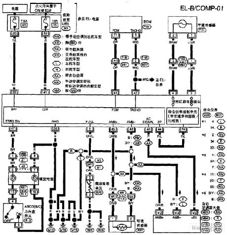
View full Circuit Diagram | Comments | Reading(497)
Nissan A32-EL warning lamp circuit 2
Published:2011/6/22 10:21:00 Author:Nancy | Keyword: Nissan, warning lamp
View full Circuit Diagram | Comments | Reading(379)
Nissan A32-EL warning lamp circuit 4
Published:2011/6/22 10:23:00 Author:Nancy | Keyword: Nissan, warning lamp
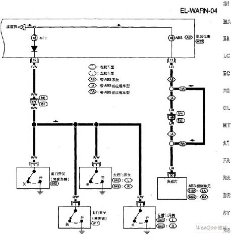
View full Circuit Diagram | Comments | Reading(372)
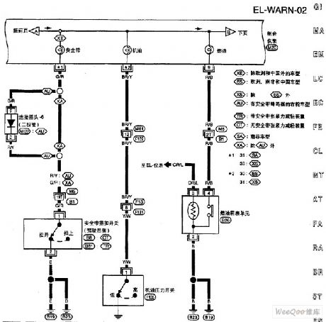
Nissan A32-EL warning lamp circuit 1
Published:2011/6/22 10:20:00 Author:Nancy | Keyword: Nissan, warning lamp

View full Circuit Diagram | Comments | Reading(384)
OPA676 programmable gain amplification circuit
Published:2011/6/20 5:37:00 Author:John
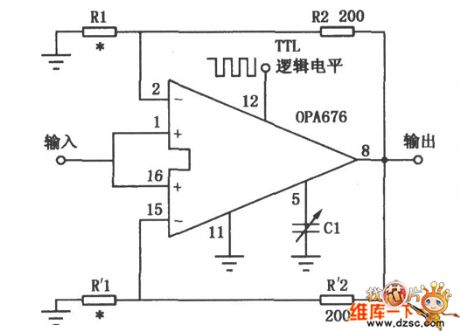
OPA676 programmable gain amplification circuit is shown.
(View)
View full Circuit Diagram | Comments | Reading(428)
Shanghai Buick Royaum V63.6L car power grounding distribution circuit diagram
Published:2011/6/24 4:32:00 Author:Nicole | Keyword: Shanghai Buick Royaum, car, power grounding, distribution
View full Circuit Diagram | Comments | Reading(444)
Shanghai Buick Royaum V63.6L car serial communication circuit diagram
Published:2011/6/24 4:33:00 Author:Nicole | Keyword: Shanghai Buick Royaum, car, serial communication
View full Circuit Diagram | Comments | Reading(376)
The stable-amplitude and low-distortion power signal generator of XG404C
Published:2011/6/13 23:59:00 Author:Borg | Keyword: stable-amplitude, low-distortion, power signal generator
In the figure is a stable-amplitude and low-distortion power signal generator of XG404C. The circuit is a good power signal source which consists of the audio power amplifier XG404. In the figure, C2, R1,C3 and R2 form a Wien-bridge frequency-selecting net, which decides the frequency of the sine wave. The leakage equivalent resistors of R3, R and FET pipe T1 determine the magnified times of the amplifier non-inverting input. When R=R1=R2 and C=C2=C3, the oscillating frequency of the circuit is f0=1/2πRC , according to the element value, the frequency is about 1kHz. (View)
View full Circuit Diagram | Comments | Reading(1392)
The oscillating circuit with the output of triangular waves and square waves (LM107、LM101A)
Published:2011/6/14 1:07:00 Author:Borg | Keyword: oscillating circuit, triangular waves, square waves
In the figure is the oscillating circuit with the output of triangular waves and square waves. This circuit consists of a Miller integrator A2 and Schmidt trigger A1, which can output triangular and square waves. The oscillating frequency is decided by the time constant of Miller integrator (R3+R4)*C1 and the lag voltage of the trigger Vcc(R1+R2)/(R1+R2+R3), of which Vcc is the power supply voltage. By adjusting the resistor R3, the oscillating frequency is also changed, and by adjusting resistor R2, either the output amplitude of the triangular wave or the oscillating frequency can be changed. A2 outputs the triangular wave and A1 outputs the square wave. (View)
View full Circuit Diagram | Comments | Reading(437)
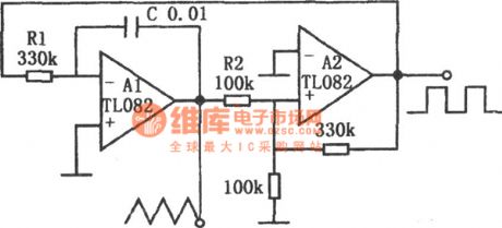
The simple square wave generating circuit of TL082
Published:2011/6/14 3:32:00 Author:Borg | Keyword: square wave, generating circuit

This circuit is a rectangular and square circuit, the time of the high/low LEV can be set separately, the oscillating frequency is decided by high and low LEV time. In the circuit, the resistors which decide the charging/discharging time of capacitor C are shifted by diodes, and the square wave high/low LEV time can be regulated by changeable resistors R1 and R2. The resistance net RA is the feedback circuit and the charging/ discharging circuit of capacitor C for the op-amp. The output voltage of the op-amp is split by the resistors of 56kΩ and 47kΩ and becomes the reference voltage, it compares with the voltage on capacitor C and then generates the oscillation. (View)
View full Circuit Diagram | Comments | Reading(1584)
The precise gated oscillator
Published:2011/6/13 20:19:00 Author:Borg | Keyword: precise, gated oscillator
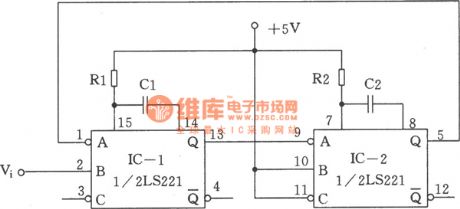
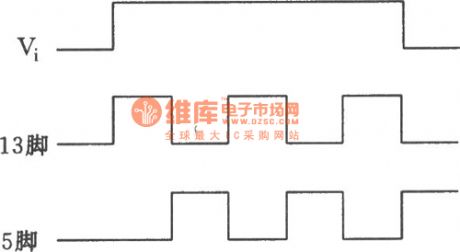
Many gated oscillator circuit generates wave of which the first period tends to be too long or too short, and not stable, too. In the figure is a gated oscillator which is made of a dual-trigger circuit 74SL221, whose wave is stable and pure, and its edge is delivered from one stage to the next stage, so it is precise. The two triggers have the same functions, and their oscillating frequencies are about l/1.4R1·Cl and 1/1.4R2·C2, the maximum value of the actual frequency is 10MHz. The wave outline circuit is as follows:
(View)
View full Circuit Diagram | Comments | Reading(536)
The auto VGA synchronized signal generator
Published:2011/6/13 20:38:00 Author:Borg | Keyword: synchronized signal generator
See as the figure, no matter what polarity of the input signal is, the circuit can generate a passive synchronized pulse. The 5v voltage which is imposed on R1 and R2 is split into two 2.5V voltages, so that we don't needed to magnify the input signal. The RC net of R3C1, which is on a OR gate terminal, can keep 2-pin in a high LEV when there is an external passive synchronized pulse, because the passive synchronized pulse is very narrow, which makes the capacitor C2 charges under the limited voltage; therefore, the pulse is no inverted. The a positive pulse is input, the LEV of 2-pin is not allowed to be raised, so the input is inverted. (View)
View full Circuit Diagram | Comments | Reading(532)
The sine and square wave generator (ICL8038、SN7473、MC1445L)
Published:2011/6/14 1:34:00 Author:Borg | Keyword: wave generator

Generally, when measuring the dynamic range and distortion of the linear amplifier, we need the sine wave; when measuring the transient state, frequency character and phase distortion, we need the square wave. This circuit has three working states, i.e sine wave output, square wave output or the auto-changed sine/square wave output. In the figure, ICL8038 is a multi-wave generator, whose output sine waves and square waves are imposed on the two poles of the video amplifier MC1445l. The square waves, which are outputed by the generator, are imposed on the counting pole of the TTL four point frequency circuit (SN7473). (View)
View full Circuit Diagram | Comments | Reading(2433)
The simple frequency multiplication generator
Published:2011/6/13 20:51:00 Author:Borg | Keyword: frequency multiplication generator
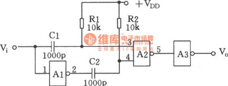
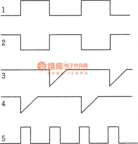
In the figure is the frequency multiplication circuit which consists of OR gates, the stepping-down edge of the input signal is differentiated by R1C1 and sent to the input terminal(3-pin) of A2, which makes A2 output a pulse, the stepping-up edge A1 is inverted and then it is sent to the input terminal(4-pin) of A2, so that A2 outputs a pulse again. As a result, by inputting a square wave, we can get two square waves at the output terminal of A2, and the frequency is doubled. A3 functions as the buffer and the rectifier. The wave outlines of the input signal are shown in the following figure.
(View)
View full Circuit Diagram | Comments | Reading(651)
The simple triangular and square wave generating circuit composed of TL082
Published:2011/6/15 21:47:00 Author:Borg | Keyword: square wave, generating circuit
In the figure is the simple triangular and square wave generating circuit composed of TL082. This circuit consists of the integrator, which is composed of computing amplifier, and the lag comparator circuit. In the figure, R1 and C form a integrating time constant, which is used to change the oscillating frequency. R2 can not only change the amplitude of the triangular wave, but also change its frequency. Besides, the oscillating frequency is effected by the output voltage of the lag comparator. Whether the output LEV is high or not is decided by the op-amp saturation and voltage. Due to the discreteness of the elements, the symmetry of the waveform is effected. (View)
View full Circuit Diagram | Comments | Reading(2949)
The ultra-low frequency triangular wave generating circuit (747、μA723)
Published:2011/6/14 0:37:00 Author:Borg | Keyword: ultra-low frequency, triangular wave
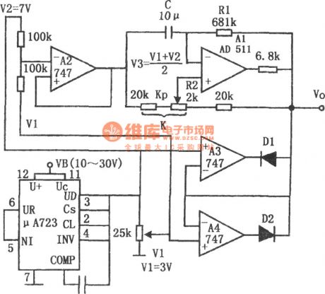
The circuit is an ultra-low frequency oscillator consisting of precise clamper circuit, which is almost a standard non-steady multi-resonance oscillator. In the figure, A3 and A4 form a symmetric precise clamper amplitude-limited circuit, with the clamper technology, the expensive voltage steady diode of temperature compensation is not needed, the feature of the circuit is that the stabilization depends only on the stabilization of the power supply voltage, and just the single polarity voltage can fulfill the dual polarity clamping. The reference voltages V1 and V2 on A3 and A4 are supplied by the reference voltage source μA723. (View)
View full Circuit Diagram | Comments | Reading(704)
The pulse frequency doubler composed of gate circuits (CD4011)
Published:2011/6/17 6:33:00 Author:Borg | Keyword: pulse frequency doubler, gate circuits
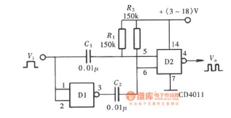
The pulse frequency doubler consists of two gates of the NAND CD4011, and one of the gates forms the phase inverter. By inputting the falling edge inverting phase of the pulse, the circuit will output a pulse with the help of the rising edge and the falling edge of the pulse, so that the aim of double frequency is fulfilled. The circuit construction is as follows.
(View)
View full Circuit Diagram | Comments | Reading(4218)
Shanghai Buick Royaum V63.6L car automatic transmission control circuit diagram(2)
Published:2011/6/24 4:14:00 Author:Nicole | Keyword: Shanghai Buick Royaum, car, automatic transmission
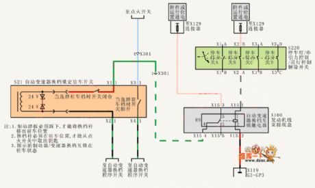
View full Circuit Diagram | Comments | Reading(389)
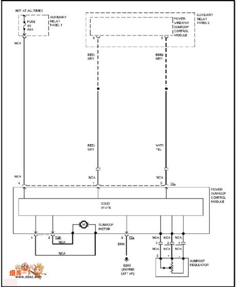
Audi awning circuit
Published:2011/6/25 11:00:00 Author:John | Keyword: awning
View full Circuit Diagram | Comments | Reading(374)
Audi door lock heating circuit
Published:2011/6/27 3:43:00 Author:TaoXi | Keyword: Audi, door lock, heating circuit

View full Circuit Diagram | Comments | Reading(410)
| Pages:67/164 At 206162636465666768697071727374757677787980Under 20 |
Circuit Categories
power supply circuit
Amplifier Circuit
Basic Circuit
LED and Light Circuit
Sensor Circuit
Signal Processing
Electrical Equipment Circuit
Control Circuit
Remote Control Circuit
A/D-D/A Converter Circuit
Audio Circuit
Measuring and Test Circuit
Communication Circuit
Computer-Related Circuit
555 Circuit
Automotive Circuit
Repairing Circuit