
Circuit Diagram
Index 322
High Voltage Converter Circuit
Published:2012/9/24 4:14:00 Author:muriel | Keyword: High Voltage, Converter


Starting from a 30 volt power supply this high voltage converter circuit can deliver a voltage between 0 to 3 kV (version 1) or from 0 to 10 kV (version 2).IC 4011 gates N1 … N3 are connected as astable multivibrator that commands the Darlington T1/T2 with an rectangular impulse of 20 kHz.The transistors cannot be brought to saturation because of the low current that goes through them which will result in a very short block period. The rapid blocking of the transistors will produse an impulse of almost 300 V in the transformer’s T1 primary winding. This voltage is multiplied by the numbers of turns from the secondary winding.
For the first version it uses a monophased rectification. The second one uses a cascade rectifier from an old TV set and it delivers a 3 times higher voltage.
3 kV/10 kV High-Voltage Converter Schematic
Version 1 and 2 of the voltage converter
IC2 LF355 regulates the output voltage by comparing the P1′s voltage with that from the common point of the voltage divider R6/R8 or R7/R8. If the output outreaches the established voltage level, IC2 will reduce the supply voltage from the output through T3.
The most important part of the high voltage converter is the transformer. You may use a variety of cores E, E+I or ferrite with 30 mm diameter. The core must not have any air gap and a value for Al of 2000 nH is pretty good. The primary winding consists of 25 turns of 0.7 … 1 mm enamelled copper and the secondary winding consists of 500 turns of 0.2 … 0.3 mm conductor. Both of the windings must have very good insulation from each other.
Regarding this high voltage converter, please remember:
capacitor C6 must support a voltage of at least 3 kV
R6 at version 1 is made of six 10 MΩ resistors in series. R7 is made of six 50 MΩ resistors in series. This is done in order to eliminate the voltage spikes.
Each circuit consumes avout 50 mA without the load and 350 mA with a 2 … 3 W load. T2 and T3 transistors need good heatsinks.
Components list of the high voltage converterR1 = 4.7KR2 = R5 = 1KR3 = 330R4 = 2.7KR6 = 60MR7 = 300MP1 = 500K
C1 = 10nC2 = C4 = C5 = 100nC3 = 1000µFC6 = 10n / 3kVC7 …. C12 = from tv module TVK 32
D1 = Zener 11VD2 = D3 = BY127D4 …. D9 = from tv module TVK 32
T1 = 2N3055T2 = BF259T3 = BU208
Tr1 = read the article
IC1 = 4011IC2 = LF355?
3 Responses to “High Voltage Converter Circuit”
(View)
View full Circuit Diagram | Comments | Reading(1625)
Electronic Lie Detector Circuit
Published:2012/9/24 4:14:00 Author:muriel | Keyword: Electronic, Lie Detector
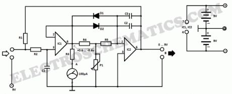
This electronic lie detector circuit will give two readings: one for difficult questions for the subject and another to show its emotional state in general.The emotional states are detected not only by heart beat accelaration and trembling hands but also an increase in skin humidity whose resistance decreases causing the entry into operation of the lie detector.Two electrodes can be used as a flexible wire, bare, wrapped around fingers or wrist.In order to not influence the measurement result the device must be powered from two 9 Volts batteries.
Each change in resistance, and therefore the voltage at the input circuit will be amplified by operational amplifier A1, which also serves as separator. The output signal will determine, by R3, a deviation of the measuring instrument.
General emotional state of a person can be assessed by measuring the average resistance of the skin over a period of time. The indication is provided by an indicator instrument connected to point B of the circuit. Operational amplifier A2 is connected as an integrator and allows the circuit to automatically adjust according to the average resistance of the skin.
Length of time to measure the skin resistance is determined by R5, C2 and C3. Until such time elapses, the lie detector gives no indication although diodes D1 and D3 provide a rapid response of the circuit.
Human skin lie detector schematic
Potentiometer P1 allows you to adjust the time delay of the circuit. Since skin resistance varies from one person to another, may be necessary to change the resistance value R1. This resistance can be replaced with a potentiometer.
Reading a great value to the instrument connected to the output of B indicates that subject’s skin resistance is low (which is a characteristic of people with sticky hands) and it is advisable to reduce the value of R1.
lie detector components listR1 = 47KR2 = 1MR3 = 3.3KR4 = 10KR5 = 10MP1 = 10KC1 = 100nC2 = C3 = 470nD1 = D2 = 1N4148IC1 = IC2 = LF356?
14 Responses to “Electronic Lie Detector Circuit”
(View)
View full Circuit Diagram | Comments | Reading(1248)
12V Battery charger circuit
Published:2012/9/24 4:13:00 Author:muriel | Keyword: 12V, Battery charger
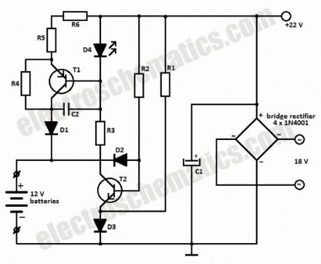


This battery charger circuit can be used to charge one or more batteries with the total nominal voltage of 12 V, meaning ten NiCd battery or six 2 V lead acid. The circuit is pretty small and can be built in a housing network adapter. The incorect usage is impossible: connecting the batteries with reverse polarity, shortcircuit of the output terminals or power loss have no impact on the charger or battery.We can use a transformer with 18 V on the secondary and then using a diode bridge to rectify the 18V ac voltage we get 22V dc on C1.
The completely discharged batteries are charged at the begining with a 6 mA current thru R2-D2 and R4-R6-D1. One the bat. have reached 0.3 – 0.5 V, the base-emitter voltage of T1 is high enough to bring the transistor in conduction.
Green LED D4 is used as an charging indicator and opens T1.There is a 60 mA current flowing thru R5-R6, this means that the charging of a 500 mAh NiCd battery will take 12 hours.
If the battery is connected with reversed polarity or there is a shortcircuit, the power transistor T1 remains blocked and the charging current can not exceed 6 – 12 mA. The current draw at maximum load is around 80 mA.
Battery charger circuit schematic
Battery charger PCB Layout
Components ListR1 = R2 = 10KR3 = 1KR4 = 5.6KR5 = R6 = 12Ω
C1 = 1nFC2 = 220µF / 35V
D1 = 1N4001D2 = D3 = 1N4148D4 = green LED
T1 = BD140T2 = BC546?
12 Responses to “12V Battery charger circuit”
(View)
View full Circuit Diagram | Comments | Reading(2928)
Solar panel to battery switch circuit
Published:2012/9/24 4:13:00 Author:muriel | Keyword: Solar panel, battery switch

When loading a battery during the day from a solar panel it can be partially discharging through the panel after nightfall. This solar panel power switch circuit replaces the diode and connects the panel to battery through a relay contact. When the power supply voltage is to low the relay is not ON, so the battery is not connected to the solar panel.When the voltage is high enough to engage the relay and the LDR receives enough light in order to open T1, the relay will switch and the battery will charge.
The relay remains ON even when the solar panel voltage starts to decrease. A battery connected and charged can not action the relay when the light intensity decreases because R2 will block T1. The brightness at which this occurs is set by P1.
Because the power consumption is determined primarily by the relay, it is important that it should a miniature one, with high coil resistance but be capable to switch up to 10 A.
Solar panel power switch schematic
Components list for solar panel to battery switchR1 = 100ΩR2 = LDR05P1 = 25KD1 = zener diode 9.1V / 1WD2 = 1N4148T1 = BC557?
7 Responses to “Solar panel to battery switch circuit”
(View)
View full Circuit Diagram | Comments | Reading(1097)
Automatic Light Switch Circuit
Published:2012/9/24 4:12:00 Author:muriel | Keyword: Automatic, Light Switch

This light sensitive automatic light switch circuit is intended to be connected at the main 220V supply. The circuit will connect a 220V lamp when at the nightfall and disconnects it in the morning light. The switching is made without a relay in order to avoid problems with the electric arc and noise caused by inductance coil and contacts.The automatic light switch is powered from the 220V network through R10, C4, D3, D2 and C3. A reference voltage source, D1, feeds with 8.2 V the circuit for measuring light, R2-P1. At lower light intensity, LDR’s resistance, R2, increases and therefore the P1 voltage falls, so will fall the gate-source voltage of FET’s T1.
When the switch S1 is closed, R3-C2 time constant makes that the gate voltage of T1 to vary slower then R2 resistance. This is necessary to prevent the circuit reaction at rapid changes of ambient light intensity.
Automatic light sensitive switch circuit schematic
T1, T2, R4, R5, R6 and R8 forms a trigger Schmitt. Normally, T1 is open and T2 is blocked. When the gate voltage of the FET goes below a certain level, T2 starts to conduct and so does T2 which will provides the necessary gate current to boost the triac Tri1 in order to connect the load (220V lamp).
Caution! Because there are many points that are connected at 220V it is essential to apply a good insolation. Do not work on the circuit when is connected to the mains.
Components listR1 = 2.2KR2 = LDRR3 = 150KR4 = 15kR5 = 10kR6 = 27kR7 = 560ΩR8 = 1.2kR9 = 1.2MR10 = 470ΩR11 = 100ΩC1 = 4.7µF/16V tantalumC2 = 47µF/16VC3 = 1000µF/16VC4 = 470nF/250V~(630V)C5 = 100nF/630VD1 = 8.2V zenerD2 = 1N4001D3 = 15V/1W zenerD4 = LEDT1 = BS250T2 = BC557BT3 = BC547BTri1 = TIC226MF1 = 5A?
18 Responses to “Automatic Light Switch Circuit”
(View)
View full Circuit Diagram | Comments | Reading(1945)
Light sensor switch circuit
Published:2012/9/24 4:12:00 Author:muriel | Keyword: Light sensor,switch


This light sensor switch circuit allows the automatic connection of a lamp when the light is low (at nightfall) and will maintain the lamp ON for a certain period of time.This time can be adjusted with P1 between 1 and 5 hours. The switch is a semiconductor relay S202DS2 and the oscillator is 4060.
Sensor light switch schematic
From the moment that T4 and T5 are opened, relay’s LED start to light and powers the lamp. As soon as one of the transistors is blocked the lamp will go OFF. The phototransistor T3 will be the one that blocks T5 if there is light that falls on T3. The T2′s base-emitter junction is connected in parallel with T3 and so will be blocked as long there is light. T2 will continuously resest IC1 whose counter outputs will be in “0″ state.
When the night falls R7 provides base current for T2 and the transistor starts to conduct. The counter can now starts to count the impulses from the internal oscillator and in this time the light will bulb will stay lit. After a time, when the output of Q13 goes in state “1″ T4 is blocked. This causes the relay’s LED to go off and the lamp too.
There is no need for external power supply because the light sensor switch is powered directly from the 220V mains. D1 … D5 diodes rectifies the voltage and C4 filters it.C5 is working as a resistor so will need to have the working voltage of minimum 400V but the 630V is preferable.
S202DS2 is a Triac-Full-Wave-Output Optocoupler produced by Sharp Electronics in a TO-220 package.
The maximum peak-to-peak voltage is 600V, max on-state current is 8 Ampere and the input trigger current is 8 mA.
Caution! This circuit is powered directly from 220V. Attention will be given for appropriate isolation of the switch block.?
7 Responses to “Light sensor switch circuit”
(View)
View full Circuit Diagram | Comments | Reading(1643)
Touch light dimmer circuit
Published:2012/9/24 4:11:00 Author:muriel | Keyword: Touch, light dimmer
With IC SLB0586A from Siemens you can build a simple touch light dimmer circuit that will allow you to adjust the lamp intensity. Together with a TIC206D triac, it enables smooth regulation of light intensity from a bulb of 10W – 400W. A coil of 100µH/5A is required to suppress switching noise.The voltage supply is obtained through R2, C2, D1 and C3 and is about 5.3V below the network potential. The touch sensor that is used to drive the IC is connected at pin 5 through two 4.7MΩ resistors, R5 and R6, in order to ensure user security.
In the adjustable touch lamp schematic we can see three selection connection , for selecting one of three modes of the IC. When the B connection is used, the light will always be ON at the last level that we used. With A or C connection the light will be ON at the minimum intensity. With B or C, the purpose of regulation is reversed with each use.
When the sensor is touched for a short period of time (50 – 400 ms), the lamp will be ON or OFF. If the sensor is touched for a longer period of time it will start the regulation process.
Schematic of the adjustable light with touch sensor
Warning! This touch light dimmer circuit has some points where lethal 220V is present, please do not try this project if you are not qualified. (View)
View full Circuit Diagram | Comments | Reading(1605)
Resistor to raise the cutoff frequency ( broadband strain signal conditioner 1B31)
Published:2012/9/23 22:54:00 Author:Ecco | Keyword: Resistor , raise, e cutoff frequency , broadband , strain , signal conditioner
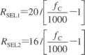

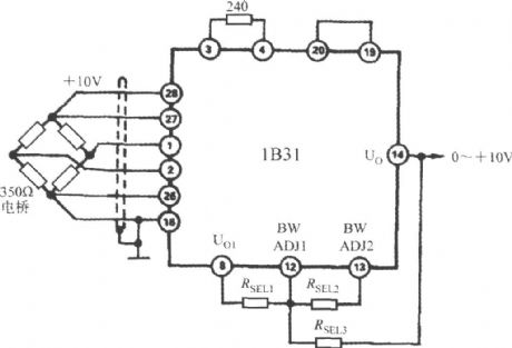
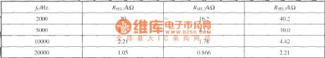
The cutoff frequency can be increased from 1kHz to 20kHz to meet the needs of broadband applications by three external resistors. The circuit is shown as the figure.
The unit of RSEL1 ~ RSEL3 istaken kΩ.The resistor valuealso can be directlyselected according to the following table.
(View)
View full Circuit Diagram | Comments | Reading(770)
Temperature controlled relay circuit
Published:2012/9/24 4:10:00 Author:muriel | Keyword: Temperature controlled, relay

This temperature controlled relay circuit is a simple yet highly accurate thermal control circuit which can be used in applications where automatic temperature control is needed. The circuit switches a miniature relay ON or OFF according to the temperature detected by the single chip temperature sensor LM35DZ.When the LM35DZ detects a temperature higher than the preset level (set by VR1), the relay is actuated. When the temperature falls below the preset temperature, relay is de-energized. The circuit can be powered by any DC 12V supply or battery (100mA min.)
Electronic Temperature-Controlled Relay Schematic
How it works?The heart of the circuit is the LM35DZ temperature sensor which is factory-calibrated in the Celsius (or Centigrade) scale with a linear Degree->Volt conversion function. The output voltage (at pin 2) changes linearly with temperature from 0V (0oC) to 1000mV (100oC).
The preset (VR1) & resistor (R3) from a variable voltage divider which sets a reference voltage (Vref) form 0V ~ 1.62V. The op-amp (A2) buffers the reference voltage so as to avoid loading the divider network (VR1 & R3). The comparator (A1) compares the reference voltage Vref (set by VR1) with the output voltage of LM35DZ and decides whether to energize or de-energize the relay (LED1 ON or OFF respectively).
Source: http://www.escol.com.my/Projects/Project-03%28Thermostat-1%29/Proj-03.html
Components list:
IC1 : LM35DZIC2 : TL431IC3 : LM358
LED1 – 3mm or 5mm LED
Q1 – General purpose PNP transistor ( A1015,…) with E-C-B pin-out)D1, D2 — 1N4148D3, D4 — 1N400x (x=2,,,,.7)
ZD1 — Zener diode, 13V, 400mW
Preset (trim pot) : 2.2K (Temperature set point)R1 – 10KR2 – 4.7MR3 – 1.2KR4 – 1KR5 – 1KR6 – 33Ω
C1 – 0.1 μF ceramic or mylar capC2 – 470 μF or 680 μF electrolytic cap. (16V min)Miniature relay – DC12V DPDT, Coil = 400 Ω or higher ?
2 Responses to “Temperature controlled relay circuit”
(View)
View full Circuit Diagram | Comments | Reading(2067)
Three - phase AC voltage regulator circuit diagram for KCZ6 component applications
Published:2012/9/23 22:41:00 Author:Ecco | Keyword: Three - phase , AC voltage , regulator, component applications

The pulse transformer can used Mn-Zn ferrite pot.It generally usesSEAR2: l pulse transformer with U30 core.
(View)
View full Circuit Diagram | Comments | Reading(4637)
The series circuit with many TcA965
Published:2012/9/23 22:51:00 Author:Ecco | Keyword: series circuit
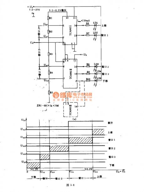
In many measuring instruments, they often require more than three of measuring ranges, and they are able to display and monitor. As shown in Figure, the series circuit composed of many window discriminators can be used. There are five ranges, i.e., three windows and an upper and a lower. They are adjusted through R1 ~ R5 dividers. Input signal UE is sent from pin 8. Figure b illustrates the pulse waveform. In actual applications, it can be used by five TCA965 connected in series.
(View)
View full Circuit Diagram | Comments | Reading(1370)
Typical Schmitt trigger circuit
Published:2012/9/23 22:29:00 Author:Ecco | Keyword: Typical , Schmitt trigger
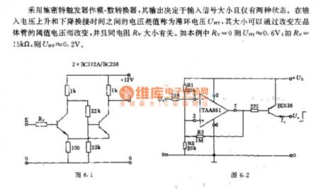
It uses Schmitt trigger for mode - digital converter, and the output depends on the input signal magnitude, and it only has two states. The voltage difference between the input voltage rising and falling the change-over time is known as the hysteresis loop voltage UNY, and its size can be changed by threshold voltage of the left transistor, and it is associated with the size of the resistance RV. Such as the present example, RV = 0 , UNY ≈ 0.6V; RV = 15kΩ, UHY ≈ 0.2V.
(View)
View full Circuit Diagram | Comments | Reading(1058)
Photosensitive monostable trigger circuit
Published:2012/9/23 22:12:00 Author:Ecco | Keyword: Photosensitive , monostable trigger
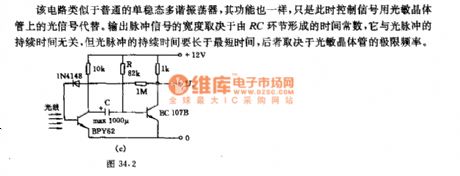
This circuit is similar to the ordinary monostable multivibrators, and their function is the same, but at this time, the control signal is replaced by optical signals on the phototransistor. The output pulse width of the signal depends on the time constant formed by the RC link, it has nothing to do with the duration of the light pulse which is longer than the shortest time, and the later depends on the limit frequency of the phototransistor.
(View)
View full Circuit Diagram | Comments | Reading(889)
Limiter and rectifier circuit using the operational amplifier
Published:2012/9/23 22:04:00 Author:Ecco | Keyword: Limiter , rectifier, operational amplifier
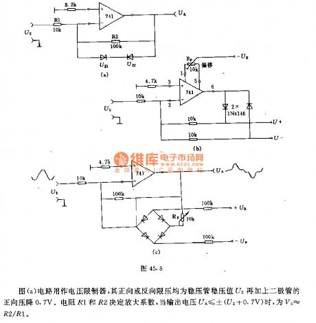
The circuit shown in Figure a is a voltage limiter, and its forward or reverse limit pressure is the zener regulator value UZ with adding 0.7V diode forward voltage drop. The resistors R1 and R2 determine the amplification coefficient, when the output voltage UA ≤ ± (UZ +0.7 V), V0 ≈ R2/R1.The circuit shown in Figure b can be used as a precision rectifier. It can output a positive or negative rectifier partial pressure according to the polarity requirements. It is often followed by the integrator in actual applications.Figure c shows the amplifier circuit with adjustable low input voltage and amplification factor. The size of dead zone can be adjusted by potentiometer.
(View)
View full Circuit Diagram | Comments | Reading(1210)
The particular application circuit of op amp
Published:2012/9/23 21:51:00 Author:Ecco | Keyword: particular application , op amp


Figure A is polarity display with two light emitting diodes, and it can be used to idendify the input signal polarity or the size of comparison signal. It uses potentiometer RP to adjust the display sensitivity oftwo light-emitting diodes.The circuit shown in figure b is used for adding several input signals UE1.UE2 and UE3.The circuit shown in Figure is a precision integrator circuit, and its RC network must match the input signal.Figure d shows a comparator circuit.The Figure e is the comparator circuit with higher frequency and the symmetrical input.Figure f is the precision comparator circuit with the voltage follower at the input termination.
(View)
View full Circuit Diagram | Comments | Reading(835)
Automatically polarity selecting electric E amplifier circuit
Published:2012/9/23 21:41:00 Author:Ecco | Keyword: Automatically , polarity selecting, electric E , amplifier

The measured voltage conversion by change-over switch is time consuming, and it is easy to generate mistake. The circuit shown in figure uses relays to automatically convert polarity. The operational amplifier 861 or 761 is used as comparator. The output voltage can control relay by the emitter follower. The relay coils is connected with a light emitting diode in series to display the selected signal.
(View)
View full Circuit Diagram | Comments | Reading(2784)
Precision rectifier circuit with integral circuit
Published:2012/9/23 21:14:00 Author:Ecco | Keyword: Precision rectifier , integral circuit
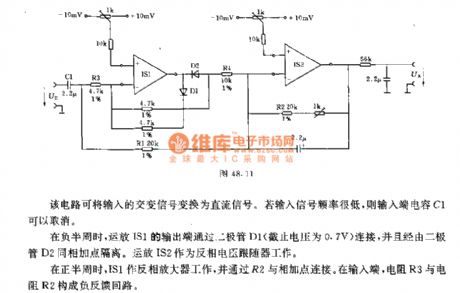
The circuit can switch input alternating signal to DC signal. If the input signal frequency is low, the input-terminal capacitor C1 can be canceled.In the negative half cycle, the output terminal of op amp IS1 is connected by diode D1 ( off voltage is 0.7V) and isolated from the same summing point via the diode D2. Op amp IS2 works as the inverting voltage follower.In the positive half cycle, IS1 works as an inverting amplifier and is connected to the summing point by R2. At the input terminal, the resistor R3 and resistor R2 constitute a negative feedback loop.
(View)
View full Circuit Diagram | Comments | Reading(1107)
Broadband voltage follower circuit
Published:2012/9/23 21:30:00 Author:Ecco | Keyword: Broadband voltage follower
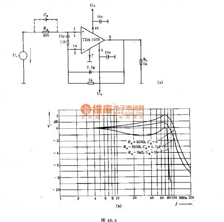
In the figure a, it is connected to frequency compensation circuit, and its amplification factor V '= 1, and it uses the full negative feedback. Small signal 3dB bandwidth frequency is 130MHz ( related to the load impedance ). If the load capacitance is large, it must be connected to resistor RD at the input end in series. Figure b shows the frequency characteristic curve of the voltage follower.
(View)
View full Circuit Diagram | Comments | Reading(781)
Homemade metal detector
Published:2012/9/24 4:09:00 Author:muriel | Keyword: Homemade, metal detector

This homemade metal detector circuit will help you find objects composed of materials with relatively high magnetic permeability. It is not suitable for buried coins discovery that is not sensitive enough but you can detect pirates treasures!
The metal detector is powered by 2 x 9V batteries, each of it charges with 15 mA. L1 detector coil is part of the sinusoidal oscillator built around transistor T1. Normally, the center frequency of the voltage controlled oscillator (VCO) from the PLL loop that is contained in IC1 is equal to the oscillation frequency of T1. This changes when entering a metallic object (ferrous or nonferrous) in the field induced by L1. S1 is a miniature 2-pole switch.Meter needle deviation is a measure of frequency change, since the direction of deviation depends on the type of material detected by the coil.The meter tool used for this homemade metal detector is zero as central, +-50µA.
Coil L1 consists of 40 turns of enamelled copper wire, wound on a plastic template with a diameter of about 10 cm. Inductance thus obtained ensure the functioning of the oscillator at a frequency approximately equal to the VCO included in the PLL loop.
Metal detector circuit schematic
Use an oscilloscope to check that pin 2 of IC1 delivers sinusoidal signal with frequency about 75 kHz. Adjust P1 so that fronts rectangular signal from pin 4 to coincide with the peaks of the sinusoidal signal from pin 2. Then, adjust P2 in order to obtain 0 on the meter. Since the neutral zero setting “runs” with the battery’s decreasing voltage it will be necessary to restore it (zero balancing) from time to time during use of the metal detector.
Related metal detector circuits?
8 Responses to “Homemade metal detector”
(View)
View full Circuit Diagram | Comments | Reading(4962)
David Moran capacitor meter project
Published:2012/9/24 4:08:00 Author:muriel | Keyword: David Moran, capacitor meter

Hi guys, I just received an email from David Moran and he sent me his capacitor meter project with pictures and a little presentation. Here are the details and schematic.
Here is the schematic of my capacitor meter I built and have used quite a bit. It will measure from zero to 0.1uf with 300pf at mid range. It is an oscillator that makes noise fed into a bridge circuit that will null out the noise when balanced. Once built, you must clip in known value capacitors and hand calibrate the dial.I built my unit into a cheap push on battery light the output can go to a small audio amp, audio input of a computer, or try a piezo speaker. The noise is rather annoying, so you may want to use a scope to view it if you must test many capacitors.
Capacitor meter schematic
And here is a picture with the finished project:
Thank you David, you’ve done a great job!?
2 Responses to “David Moran capacitor meter project”
(View)
View full Circuit Diagram | Comments | Reading(1428)
| Pages:322/2234 At 20321322323324325326327328329330331332333334335336337338339340Under 20 |
Circuit Categories
power supply circuit
Amplifier Circuit
Basic Circuit
LED and Light Circuit
Sensor Circuit
Signal Processing
Electrical Equipment Circuit
Control Circuit
Remote Control Circuit
A/D-D/A Converter Circuit
Audio Circuit
Measuring and Test Circuit
Communication Circuit
Computer-Related Circuit
555 Circuit
Automotive Circuit
Repairing Circuit