
Circuit Diagram
Index 329
220V blinking LED circuit
Published:2012/9/18 21:23:00 Author:Ecco | Keyword: 220V , blinking LED
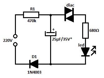
This is a simple blinking led circuit powered from 220V that can be used to mark special places or as voltage indicator. The voltage from the mains charges the capacitor through R1 resistor and D1 diode.
As long as the capacitor’s voltage doesn’t exceeds the diac’s switching voltage the cap is acting as a blocked diode. After reaching the switching voltage the diac is conducting and the cap’s discharging current lights up the LED.The blinking frequency of the LED depends mostly on the RC time constant (in this case T = 11 seconds). The capacitor’s voltage must be a little bit higher than the diac’s breakover voltage.
220 volts blinking LED schematic
With a 1N5758 diac the triggering voltage will be at 20V ± 2.?
5 Responses to “220V blinking LED circuit”
(View)
View full Circuit Diagram | Comments | Reading(2710)
12V Battery checker circuit
Published:2012/9/18 21:23:00 Author:Ecco | Keyword: 12V, Battery checker


This is a 12V battery checker circuit that uses 3 LEDs that light up at their respective voltages. The red LED lights up when the battery voltage is between 8 to 10V, the orange one at voltages between 10.5V to 12V and the green one when the battery voltage is above 12.5V.This is a tried and tested battery checker circuit using one NPN and one PNP transistor. A PCB is given along with the schematic.
6 Responses to “12V Battery checker circuit”
(View)
View full Circuit Diagram | Comments | Reading(2572)
12V battery level indicator circuit
Published:2012/9/18 21:22:00 Author:Ecco | Keyword: 12V, battery level indicator
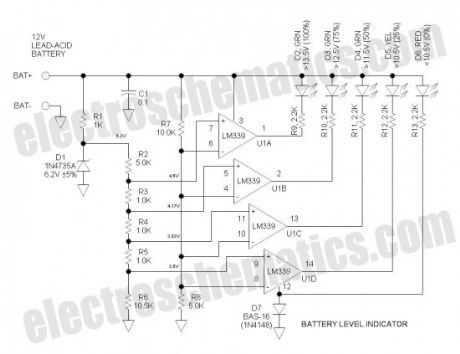

This battery level indicator offers (5) LEDs that light up progressively as the voltage increases:
Red: Power Connected (0%)
Yellow: Greater than 10.5V (25%)
Green 1: Greater than 11.5V (50%)
Green 2: Greater than 12.5V (75%)
Green 3: Greater than 13.5V (100%)
Of course, you may select your own colors if desired.
12 Volts Battery Level Indicator Circuit Schematic
Operation of the battery level indicator
D1 is the voltage reference zener. Tied to this is a string of divider resistors (R2-6) that set the various fixed voltage levels. R7 & 8 form a voltage divider to that reduces the battery voltage by a factor of 3. U1 is an LM339 quad comparator that compares the various voltages from the two dividers. The comparator sections have open collector outputs that simply function as switches to operate the LEDs. D7 protects against reverse battery connection.
The LEDs are biased to operate at about 4mA which is quite bright if modern LEDs are used. This current can be adjusted simply by varying the series resistors (R9 through R13). The overall current drain as shown is about 25mA which tends to be wasteful for continuous operation. For energy conservation, connect to battery via a pushbutton (Push to Test).
Printed Circuit Board
I did a www.expresspcb.com SMT layout using 0805 size components, 1N753 zener and SOIC-14 IC. D7 is in a SOT-23 package. These components are about as small as I like to work with. The layout has not yet been carefully checked or built. Note that surprises abound when constructing prototypes.The circuit board measures only 0.5” x 1.5”.
More recently, I located an inexpensive SOT-23 zener with a 2% voltage tolerance—this has not yet been incorporated.
I have had good results with 0805 size LEDs purchased from China on eBay. They are both inexpensive and BRIGHT!
The 12v battery level indicator unit in the photo has no reverse polarity diode and R2 is the calibration potentiometer.
6 Responses to “12V battery level indicator circuit”
Source: electroschematics.com
(View)
View full Circuit Diagram | Comments | Reading(2452)
Light activated switch
Published:2012/9/18 21:22:00 Author:Ecco | Keyword: Light activated switch
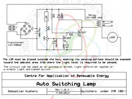
The circuit can be used for switching OFF a particular lamp or group of lamps in response to the varying ambient light levels. The unit once built can be used for switching OFF a lamp when dawn breaks and switching it ON when dusk sets in.
The power supply is a standard transformer, bridge, capacitor network, which supplies a clean DC to the circuit for executing the proposed actions.
Automatic light activated switch circuit schematic
The LDR must be placed outside the box, meaning its sensing surface should be exposed toward the ambient area from where the light level is required to be sensed. The circuit can be used as an automatic street light controller system or a simple light activated switch.
24 Responses to “Light activated switch”
(View)
View full Circuit Diagram | Comments | Reading(724)
Pathway Lighting with LEDs
Published:2012/9/18 21:22:00 Author:Ecco | Keyword: Pathway Lighting , LEDs

Simple pathway lighting that would provide illumination for the path at night. Extension for the Solar garden Light. The torroid is bifilar wound. The Torroid is 10mm and Cat 5 cable is wound around the same.
Solar panels of 3.5 maybe difficult to procure using 2 2V panels in series could be used. If you do use 4V panel then suggest you add another diode in series with 1N4001 to drop voltage to contain voltage to the battery.
The characteristic voltage for a white LED is 3.2V but the addition of the torroid provides the boost to drive the white LED. If you cannot procure the battery as suggested you can use 600 mAH battery then do not go above 3/4 LED’s.
Pathway LED Lights Schematic
?
7 Responses to “Pathway Lighting with LEDs”
(View)
View full Circuit Diagram | Comments | Reading(1845)
Car Battery Charger with transistors
Published:2012/9/18 21:21:00 Author:Ecco | Keyword: Car Battery Charger , transistor

This car battery charger circuit can be used to charge 12V and 6V batteries. If it is used a transformer that can deliver 4A to 5A at a voltage between 12.6V and 16V then we can get rid of the switch for 6V or 12V batteries.
12V car battery charger circuit schematic
The car battery charging current is automatically limited to 4.2A. If there is a 600mV voltage on R1 (4A thru it), then the T1 transistor starts to conduct. Excessive charging current is avoided because the current value on T3′s base is limited. The difference between applied load current (at T4′s collector) and real voltage of the battery is balanced thru T4′s collector-emitter junction.
The power input of T4 (2N3055) is the product of load current and voltage difference already mentioned. When charging 6V car battery this power reaches a maximum of 40W. The rectifier diodes must be able to deliver 4A at 40V. T4 2N3055 must be mounted on a good heatsink in order to dissipate the heat.?
2 Responses to “Car Battery Charger with transistors”
Source: electroschematics.com
(View)
View full Circuit Diagram | Comments | Reading(3043)
Sine to rectangular wave conversion circuit
Published:2012/9/18 21:21:00 Author:Ecco | Keyword: Sine to rectangular wave , conversion
We have already given many posts on Op-Amp circuits. But the list of applications of Op-Amp will be keep on going. ?The best Op-Amp circuit which is used to convert sine waveform into rectangular waveform is the schmitt trigger circuit.To avoid the false triggering, a positive feedback is used in a comparator circuit of an Op-Amp. Thus the comparator with positive feedback is called Schmitt trigger or regenerative comparator. The inverting schmitt trigger mode produces opposite polarity output. This is?fed back to the non-inverting input which is of same polarity as that of output. This ensures positive feedback.
The above shown schematic is the sine to rectangular conversion circuit. For proper conversion of input signal from sine to rectangular, the input must be large enough to pass through both the tripping voltages.
When the input signal is periodic, for any shape of the input signal, the Schmitt trigger always produces rectangular waveform.
Practically sometimes a capacitor C1 is connected in parallel with R1, as shown in the above schematic. The stray capacitance C2 forms the bypass circuit with R2. The use of speed-up capacitor C1 across R1 eliminates the effect of stray capacitance C2. Without speed-up capacitor, the stray capacitance C2 is required to be charged before the non-inverting input voltage changes. The speed-up capacitor used supplies the necessary charge to C2. For neutralizing the effect of stray capacitance, the minimum value of speed-up capacitor must be,
C1(min) = (R2/R1) C2.
When C1 is selected is greater than C1(min) then the switching of the output is very fast.
The frequency of the output of the Schmitt trigger is same as the frequency of the input signal.
The peak to peak value of the output rectangular waveform is approximately 2Vsat. (View)
View full Circuit Diagram | Comments | Reading(674)
Sleep Aid in case of insomnia
Published:2012/9/18 21:18:00 Author:Ecco | Keyword: Sleep Aid, in case of, insomnia
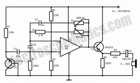
Insomnia treatment consist mostly of sleeping pills consumption but this circuit is an alternative for that and consists of a simple circuit that generates a rain sound effect. The japanese researches were the first to discover that sound of rain has a relaxing effect. With the help of this simple circuit we can generate the rain sound which can be a sleep aid in case of insomnia.T1 is used as a noise generator and its signal is amplified by the 741 IC and thru T2, R7 and C4 goes to a headset with low resistance. If you do not want to use the headphones then use a speaker with impedance between 4 and 16 Ω. With the help of P1 can adjust sound level and with P2 the tone.
Sleep Aid Circuit Schematic
?
5 Responses to “Sleep Aid in case of insomnia”
Source: electroschematics.com
(View)
View full Circuit Diagram | Comments | Reading(1892)
Firefly Lights Circuit
Published:2012/9/18 21:17:00 Author:Ecco | Keyword: Firefly Light


This firefly lights flasher is an easy, fun project.It can be built on the tiny circuit board, or on perf board.
Specifications
Battery life: approx 1year using the NXP 7555 CMOS timer IC & standard alkaline battery, or about 6months using the more common TI TLC555
Flash rate: approx 0.25hZ (unless using optional potentiometer)
Dimensions: 14.5mm2
Minimum voltage: approx 6V
Firefly flasher circuit schematic
Bill of Materials (if on perf board, use standard through-hole rather than SMT components)
PCB ExpressPCB.com
U1 NXP 7555 or TI TLC555 Timer IC, SOIC-8
R1 10K, 0805
R2 2M, 0805
R3 Potentiometer, 1M , 0.2” lead spacing (optional)
C1 10uF, 25V, X7R, Ceramic, 0805
D1 Diode, BAS16, or MMBD4148, SO23-3
D2 LED, Green, High Brightness, 0805
Battery Standard 9V
How the firefly lights works
It functions like almost any 555 astable timer, except that the LED is inserted into the capacitor reset path so that when pin 7 discharges C1 to common, this relatively high current must pass through the LED. In this way, the average battery current is only about 100uA. When battery voltage becomes very low, the LED threshold voltage prevents discharging C1 down to the lower threshold—when this happens, R2 finishes off the discharge because the output switches to ground potential the same time pin 7 turns on—you will find that this works on almost dead batteries that may be useless for other applications. D1 protects against accidental reverse battery voltage.
Background
Fireflies are common through Northeastern US and also in many other parts of the world. This green LED has the same color, flashes at about the same duration and has a similar repetition rate just like a real firefly (lightning bug). Put a number or these around your grounds and they will truly resemble fireflies—there will be no synchronization of the flashes. The only thing this cannot do is to fly—fireflies ascend as they flash, and they do not flash when perched to protect from predators. Also, this is much larger than the tiny firefly beetle that measures about 3 x 20mm.
Photographs
Visible on the photo is a wire jumper connecting R2 to IC pin 3. This was an afterthought when I found that low voltage operation was poor. The PCB file is updated to fix this. The optional resistor is not used in this case, but is easy to add if desired. You may adjust component values to obtain desired results.
For the Future
Make it extinguish during daylight hours thus doubling battery life to 2years.
Happy experimenting!
2 Responses to “Firefly Lights Circuit”
Source: electroschematics.com
(View)
View full Circuit Diagram | Comments | Reading(1272)
12V LDO Solar Charge Control
Published:2012/9/18 21:16:00 Author:Ecco | Keyword: 12V , LDO , Solar Charge Control

This Low Dropout Voltage (LDO) solar charge control uses a simple differential amplifier and series P channel MOSFET linear regulator—their compatibility seems like a marriage made in heaven. Voltage output is adjustable. It is mainly intended for charging 12V lead-acid batteries.Solar Charge Control Specifications
Solar panel rating: 50W (4A, 12V nominal) (open circuit voltage: 18 to 20V)
Output voltage range: 7 to 14V (adjustable) (not recommended for 6V applications)
Max power dissipation: 16W (includes power dissipation of D3)
Typical dropout voltage: 1.25V @ 4A
Maximum current: 4A (current limiting provided by solar panel characteristics)
Voltage regulation: 10mV (no load to full load)
Battery discharge: 1mA (Chinese controls discharge at typically 5mA)
LED indicators:
RED: Solar panel active
GREEN: Series regulator limiting current (fully charged or topping off)
Reverse battery protection: Control shuts down if battery is inadvertently connected reverse
12V Solar Charge Control Schematic
Bill of Materials
In Excel format (download link at the bottom)
Dropout Voltage
The input voltage exceeds the input voltage by 1.25V when charging at the maximum rate—the lower, the better. Low Dropout Voltage (LDO) is the catch phrase for anything under approximately 2V. This could potentially be reduced to below 1V by making D3 a schottky rectifier.
Current Limiting
Current limiting is provided by the solar panel—it is not a commonly understood fact that the solar panel tends to be a constant current device. For this reason, a solar panel can withstand a short circuit. Therefore, the control does not need current limiting.
Float Charge of Lead-Acid Batteries
This control charges the battery at a constant voltage and also maintains a charged battery (float charge). The float charge voltage specification is a little lower than the charge voltage, so to accommodate both voltages, a compromise is reached by simply reducing the voltage slightly—that is how ALL automotive systems operate. To obtain maximum charge in a 12V battery, set the control to 14 to 14.6V. Automotive systems further reduce voltage to 13 to 13.5V in order to accommodate high temperature operation as the battery is usually located in the hot engine compartment—battery has a negative thermal coefficient of voltage.
Voltage Adjustment
To set the voltage, disconnect the battery and connect a 1K dummy load resistor to the output. The resistor is necessary to shunt potential MOSFET leakage current as well as the green LED current.
LDO Solar Charge Control Circuit Operation
R4 and D1 form a 6V shunt zener voltage reference. Q1 & Q2 make up the classic differential amplifier that amplifies the difference between the reference voltage and the feedback voltage from the arm of potentiometer R6. The output is taken from the collector of Q2 and drives the gate of P Channel MOSFET Q3. Differential voltage gain is probably in the order of 100 to 200. For best performance, I selected Q1 & Q2 for matched hFE. As the feedback voltage increases at the arm of R6, Q2 turns on harder and steals some of the emitter current away from Q1. The collector current of Q1 follows the emitter current and drops less voltage across R1 thus reducing Vgs of Q3 and turning it off. C2 provides frequency compensation to pr
Source: electroschematics.com (View)
View full Circuit Diagram | Comments | Reading(2839)
Programmable Unijunction Transistor Flasher
Published:2012/9/18 21:15:00 Author:Ecco | Keyword: Programmable Unijunction , Transistor Flasher


This is simple circuit that illustrates the function of the programmable unijunction transistor. It may be quickly wired on a proto-board.
PUT Flasher Specifications
Flash rate: approx 1hZ
Load current: approx 300uA
Minimum voltage: approx 4V
PUT Flasher Circuit Schematic
How it works
The programmable unijunction transistor remains dormant until the voltage across C1 exceeds the gate voltage of Q1 by one diode drop (0.6V) or in this circuit about 6.8V in reference to circuit common. At this point, current starts to flow into the anode of Q1. When the current exceeds the “peak current” threshold (about 1.25uA), the transistor triggers and shorts all three terminals together until the anode current drops below the “valley current” (about 100uA in this case), and the transistor resets itself. When the transistor triggers, it dumps capacitor C1 across the LED. Peak current is limited by the LED internal resistance.
By varying (programming) the gate voltage, the voltage at which the transistor fires varies—in this case, it varies the flash rate.
Background
This cute little device was developed by General Electric about 50years ago. The original GE part numbers were D13K1 and D13K2 (now 2N6027 and 2N6028). The 2N6028 has tighter specifications for more precision applications. On Semiconductor is now the sole manufacturer, but NTE has a relatively expensive equivalent device.
PUT Applications
There are many, many applications for this device, but it is mainly useful for triggering thyristors. Other than for thyristor triggering, the ubiquitous 555 timer has taken over.
Photographs
Proto-board circuit layout
For the Future
Use of this device in a thyristor switch circuit
Bill of Materials
Q1 On Semiconductor 2N6027 (comes only in T0-92 package)
R1 100K
R2 10K
R3 22K
C1 10uF, 25V aluminum electrolytic
D1 LED Red, High Brightness
Battery Standard 9V ?
One Response to “Programmable Unijunction Transistor Flasher”
(View)
View full Circuit Diagram | Comments | Reading(2253)
Security Light & Switch with PIR Sensor Update
Published:2012/9/18 21:15:00 Author:Ecco | Keyword: Security Light, Switch , PIR Sensor Update
This is a simple update to Mr. Hareendran’s PIR Sensor Security Light circuit. It has a shortcoming limits the relay voltage to approximately 3.3V. While this may function with some 5V relays, it will not function with all. The nature of an emitter follower Darlington forces the output voltage to be two junction drops below the base drive voltage plus a small voltage drop across R1.In keeping with the spirit of his design, I retained the Darlington arrangement, and the transistor type number—however, I changed the transistors from common collector to common emitter configuration, and connected the relay between the collector output and the positive rail. The relay now utilizes a 12V coil—to use an existing 5V relay, simply add a resistor in series with the coil whose value is scaled up from the coil resistance. Also, I connected the LED across the relay coil rather than powering it via the 2nd relay contact—this way, only one form “C” relay contact is required thus making the relay less expensive—of course it can be done either way. I eliminated some additional, unneeded components.
Security Switch & Light Circuit Schematic
Datasheet links
SB0061 PIR Sensor (complete PIR module):epled-2008.en.made-in-china.com/BISS0001 PIR Sensor (interface IC that goes inside many PIR modules):http://www.ladyada.net/media/sensors/BISS0001.pdf
How it works
When motion is detected, the output (pin 2) goes to 5V and current flows through R2 to the base of Q1. The emitter current of Q1 becomes the base current of Q2—the current gain of a Darlington is the hFE squared or about 10,000 to 50,000 (very high). This easily provides adequate drive current for the relay. R1 provides a means of conducting any potential leakage in Q1 to common and also helps Q2 to turn off faster. D1 is the back diode that circulates the relay coil current when Q1 & Q2 turns off thus preventing a damaging voltage transient.
Testing
No, I did not build and test this one—I just happen to know from experience that this circuit will work OK—if the circuit was new to me, I would definitely Protoboard and test because Murphy may be lurking somewhere. Murphy’s Law states that anything that can go wrong will go wrong… Such is true as I have proven it numerous times.
For the Future
PIR crystal amplifier circuit—yes, it is not difficult. (View)
View full Circuit Diagram | Comments | Reading(1464)
Photocoupling zero-crossing control socket circuit using TWH9205
Published:2012/9/18 2:34:00 Author:Ecco | Keyword: Photocoupling , zero-crossing control , socket
As shown in Figure, the circuit consists of zero-crossing driving switch, photoelectric coupling input circuit, the thyristor control circuit and sound circuit. The phototransistor switching circuit in FIG is connected to the inverting input terminal ( 9 feet) of the differential switching amplifier TWH9205, when the terminal voltage is lower than the clamping voltage of the positive-phase input terminal, i.e., when the phototube 3DU5 is irradiated by light, only when AC os over zero, TWH9205 outputs high to drive SCR VS conduction, then socket XS gets electric, and the electrical equipments connected to XS operate. VS can use 1 ~ 500A triac according to the size of the electrical load power.
(View)
View full Circuit Diagram | Comments | Reading(1200)
Single-phase motor two-speed circuit with auxiliary winding connecting to tap directly
Published:2012/9/18 2:16:00 Author:Ecco | Keyword: Single-phase motor , two-speed circuit, auxiliary winding , tap

As shown in the figure, the circuit uses stator on the auxiliary winding LA to directly connect totap forspeed adjusting, and it has no governor winding.
(View)
View full Circuit Diagram | Comments | Reading(2809)
The AC contactor saving and silent running circuit 1
Published:2012/9/18 1:36:00 Author:Ecco | Keyword: AC contactor, saving , silent running
In the circuit shown in figure, when the motor is starting, pressing the start button ST, AC contactor KM will pull in, then the KM auxiliary contacts are closed; releasing the ST, ST normally closed contact will restore the closed state, then the diode VD and KM coils are connected in parallel, and KM self-locking contact connects to the power supply through a capacitor C, KM turns to DC operation. Capacitor C plays buck role in the circuit and makes the AC are flows from top to bottom of coil in the positive and negative half-wave, and it changes AC contactor to DC operation. DC operating noise is minimal, so it is also called AC contactor silent running.
(View)
View full Circuit Diagram | Comments | Reading(985)
The voice control flowing Lantern associated with many famous songs circuit ( 5G167 )
Published:2012/9/18 1:42:00 Author:Ecco | Keyword: voice control , flowing Lantern , many famous songs

As shown in the figure, the circuit consists of acoustic / electric sensor, audio amplifier, ring count pulse distribution / driver circuit, SCR control circuit, songs sound circuit, audio amplifier circuit and AC buck rectifier circuit. IC1 uses 5G167, it is designed for ring count pulse distribution / driver ICs used in tape recorders rotary flash box, it contains the signal rectifier amplifier, voltage controlled oscillator and 3-bit ring timing counter and 3 drain output circuits and so on.
(View)
View full Circuit Diagram | Comments | Reading(722)
Triac governor circuit
Published:2012/9/18 1:48:00 Author:Ecco | Keyword: Triac governor

The motor M and TRIAC VS are connected in series, if changing the conduction angle of the VS, the AC voltage applied to both ends of the motor M can be changed to realize stepless speed adjust in the range of 0 ~ 220V. General Triac trigger circuit is more complex with a lot of components. The circuit shown in figure only uses a potentiometer RP to achieve speed control purposes. It uses equipotential trigger circuit , i.e. whether it is a positive trigger or a negative trigger, the control electrode G and the potential of the cathode of T2 are the same. This circuit can be used the governor in fan, incandescent dimmer or other household appliances.
(View)
View full Circuit Diagram | Comments | Reading(2711)
Bathroom door control switch circuit ( 2 )
Published:2012/9/18 2:04:00 Author:Ecco | Keyword: Bathroom , door control switch

The circuit is used to control the bathroom lights and exhaust fan. When someone opens the door and comes to the bathroom, the door control switch is turned on, the bathroom light will be lit and exhaust fan is also energized; When users open the door and come out of the bathroom, the door control switch is turned off, lights will be turned off, the exhaust fan is also interrupted.The bathroom door control switch circuit inlcudes the power circuit, monostable flip-flop, flip-flop circuit and control execution, and it is shown in the figure.
(View)
View full Circuit Diagram | Comments | Reading(1264)
Bedside lamp safety switch circuit (2)
Published:2012/9/18 1:50:00 Author:Ecco | Keyword: Bedside lamp, safety switch

Thebedside lamp safety switch shown in the figure uses Triac. RL should use photoresistor with light resistance beingless than 2kΩ.
(View)
View full Circuit Diagram | Comments | Reading(1189)
DC / DC converter circuit diagram using six inverter
Published:2012/9/18 2:28:00 Author:Ecco | Keyword: DC / DC converter , six inverter
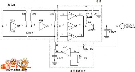
The circuit can be used to adjust voltage by TTL switch threshold. U1A and U1B form the oscillator, and its switching frequencies < 1MHz. The output of the oscillator can drive the three parallel inverters U1C, U1D U1E to provide a higher output current and output power. Its internal output transistor, L1 and D1 form a standard boost converter, when its output is low, the current only flows through the inductor L1; when the output becomes high, the energy stored in the inductor makes anode of D1 become high, D1 conduction charges for C1. The circuit and load characteristics are better than 1%, and output voltage only changes 7% in range of 0 ℃ ~ 50 ℃.
(View)
View full Circuit Diagram | Comments | Reading(943)
| Pages:329/2234 At 20321322323324325326327328329330331332333334335336337338339340Under 20 |
Circuit Categories
power supply circuit
Amplifier Circuit
Basic Circuit
LED and Light Circuit
Sensor Circuit
Signal Processing
Electrical Equipment Circuit
Control Circuit
Remote Control Circuit
A/D-D/A Converter Circuit
Audio Circuit
Measuring and Test Circuit
Communication Circuit
Computer-Related Circuit
555 Circuit
Automotive Circuit
Repairing Circuit